Tunable dual-band terahertz graphene absorber with guided mode resonances*
2021-01-21JunWu吴俊XiaYinLiu刘夏吟andZheHuang黄喆
Jun Wu(吴俊), Xia-Yin Liu(刘夏吟), and Zhe Huang(黄喆)
1Department of Physics,Zhejiang University of Science and Technology,Hangzhou 310023,China
2College of Electrical Engineering,Anhui Polytechnic University,Wuhu 241000,China
Keywords: dual-band,graphene,guided mode resonance,spectrum selective absorption
1. Introduction
In recent years, the terahertz (THz) frequency range(0.1 THz–10 THz) has attracted increasing attention due to its potential applications in communication, imaging, spectroscopy, biomedicine, etc.[1–3]Many attempts have been made to develop the THz devices, among which the THz absorbers have been extensively studied. They have been widely used in detectors,[4]thermal emitters,[5]biological and chemical sensors,[6]modulators,[7]stealth devices,[8]etc.Therefore, the enhancement of absorption at the THz band is significant for realizing the THz devices. Traditionally,THz absorbers can be designed by using metallic metamaterials, among which different kinds of structures have been proposed to realize various absorption functions including multi-band,[9,10]broadband,[11,12]and absorbing frequency tuning.[13]However, it is still required to search more methods to combine novel material into metamaterials to realize the THz absorbers with more engineered absorption functions.
Fortunately, graphene, a two-dimensional material consisting of one monolayer of carbon atoms, has emerged as a promising, alternative candidate for THz applications due to its extraordinary electric, optical, mechanical, and thermal properties.[14–16]Owing to the two dimensional feature of graphene, graphene can excite strong surface plasmon polaritons with tight field confinement.[17]In addition, its electric conductivity can be continuously tuned in a broad frequency range.[18]These properties make graphene extend its applications in perfect absorption,[19,20]modulation,[21]biosensing,[22]photodetection,[23]optical phase modulation,[24]plasmonic waveguides.[25]Unfortunately, due to graphene being atomically thin, the interaction between the graphene and light is usually extremely weak. Thus, the enhancement of absorption in graphene monolayer plays a key role in realizing the graphenebased Thz devices. Various methods have been proposed to enhance the absorption in graphene, such as graphene metasurface-spacer layer-metallic mirror structure,[19,20]critical coupling with a photonic crystal guided resonance,[26]guided mode resonances,[27–29]ultrasensitive absorption in graphene based on bound states in the continum,[30]etc.However, these absorbers are usually operated in a single-band resonance.[19,20,26–30]
In this paper,a tunable dual-band terahertz absorber is designed and investigated. It is achieved by placing a graphene monolayer on a guided-mode resonant filter. The absorption properties of the graphene absorber are investigated by the rigorous coupled-wave analysis (RCWA),[31,32]which is achieved by our home-made code with the number of harmonics being 50. The electric field intensity distribution is illustrated to disclose the physical mechanism of such a dual-band absorption phenomenon. In addition, the influence of geometric parameter on the absorption spectrum is studied,which will provide useful guidance for fabricating this absorber. Finally,the influences of optical properties of graphene,including Fermi level and relaxation time, on the absorption spectrum are investigated.
2. Design and results
The proposed structure of the dual-band THz absorber is presented in Fig. 1(a), which consists of a graphene monolayer supported by a one-dimensional(1D)guided-mode resonant filter. The 1D guided-mode resonant filter is composed of a dielectric grating loaded with a dielectric film and an antireflection film on a substrate. In Fig. 1, d is the period of dielectric grating,h,w,and hgare the depth,width,and thickness of graphene, respectively; hfand hARare the thickness of dielectric film and antireflection film,respectively. The refractive indexes of grating ridge and groove are nH=1.5 and nL=1.0,respectively.The refractive indexes of dielectric film and antireflection film are nf=1.7 and nAR=sqrt(nf·ns),respectively,where ns=1.47 is the refractive index of substrate.A TE polarization (with electric field parallel to the y direction) monochromatic plane wave is incident from air at incident angle θ.

Fig. 1. Schematic diagram and geometric parameters of the proposed graphene absorber.
The complex surface conductivity of graphene can be calculated from σ(ω) = σinter(ω)+σintra(ω), where σinter(ω)and σintra(ω)are the interband contribution and intraband contribution,respectively. At room temperature T =300 K and in the THz range,the interband transitions are negligible,hence the conductivity σ(ω)can be approximated as[33,34]
where Efis the energy of Fermi level,is the reduced Planck’s constant,ω is the angular frequency,τ is the carrier relaxation lifetime, and e is the elementary charge. The relaxation time and Fermi level are initially considered to be τ =0.3 ps and Ef=0.5 eV, respectively. Their influence on absorption performance will be analyzed latter.
In the simulation,the graphene is modeled as a thin layer with a thickness(hg)of 0.34 nm with an equivalent dielectric constant
where ε0is the relative permittivity of vacuum.
The optimized geometric parameters of the unit cell are listed as follows: dx=31.5 μm, w=28.8 μm, h=10 μm,hf=34.3 μm, and hAR=7.51 μm. In Fig. 2, we show the absorption spectra corresponding to normally incident TE polarizations light. The absorption spectrum A(λ) is calculated from A(λ)=1-R(λ)-T(λ),where R(λ)and T(λ)are the corresponding reflection spectrum and transmission spectrum,respectively. It is found that two absorption peaks are obtained at f1=5.8245 THz(A1=41.54%)and f2=6.386 THz(A2=45.45%),which exhibits that the absorption is enhanced by approximately 18 and 20 times compared with the absorption in monolayer graphene (2.3%), respectively. Moreover,the full width at half maximum (FWHM) of the two absorption peaks are about 0.001 THz and 0.0025 THz,respectively,both exhibit ultranarrow linewidth. In Fig.2,we can also see the absorption spectrum for TM polarization (with magnetic field parallel to y-direction). Though the structure parameters are optimized for TE polarization, two absorption peaks are also achieved for TM polarization,only with reduced peak absorption. Without loss of generality,we only consider the case of TE polarization below.
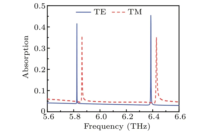
Fig. 2. Normal-incidence absorption spectra of graphene in the frequency range from 5.6 THz to 6.6 THz.
In order to intuitively confirm the dual-band absorption mechanism,the normalized electric field distribution|Ey/E0|2at frequencies f1and f2are calculated and shown in Figs.3(a)and 3(b), respectively. The origin of the z axis is located at a surface 10 μm below the antireflection film. Figures 3(a)and 3(b) clearly show that the different absorption frequencies correspond to the different electric field patterns. From Fig.3(a),it is found that the strong electric field intensity enhancement and concentration for frequency f1are merely presented in the dielectric film. However, the electric filed intensity of frequency f2is enhanced and concentrated in the dielectric film and the antireflection film. For both resonant frequencies, the electric field intensity distributions present standing wave profiles in the x direction, which is a typical feature of guided mode. For a nonmagnetic dispersive medium, the time-averaged power loss density is calculated from[35]dPloss/dV =(1/2)ε0ω Imε(ω)|E|2,where ε0is the permittivity of vacuum,ω is the angular frequency,Im(ε)denotes the imaginary part of relative permittivity and E denotes the electric field. Therefore, the graphene monolayer located on the dielectric grating with a strong electric intensity enhancement will result in the enhancement of absorption in the graphene monolayer. The enhanced absorption in graphene monolayer at different frequencies is attributed to the general guided mode resonances with different mode numbers.
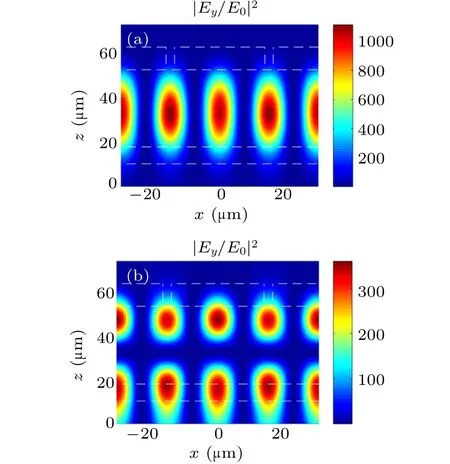
Fig. 3. Electric field intensity distribution of |Ey/E0|2 at (a) f1 and (b) f2,respectively. Regions enclosed by white dash line are dielectric grating, dielectric film, and antireflection film. A graphene monolayer is placed on dielectric grating and it cannot be displayed due to its ultra-thin thickness.
3. Discussion
In general,the changes in the structure parameters should have a direct effect on the dual-band absorption performance,which can be employed first to tune the resonant frequencies of both absorption peaks. The absorption spectra as a function of d, w, h, hf, and hARare shown in Figs. 4(a)–4(e), respectively. As shown in Fig. 4(a), both absorption peaks exhibit a red shift with the increase of grating period. Similarly,when w increases,both peaks of absorption present red-shifts as illustrated in Fig. 4(b). In addition, the second absorption peak has a larger red-shift than the first absorption peak. As can be seen by comparing Fig. 4(a) with Fig. 4(b), the influence of d on absorption peak is larger than that of w. From Fig. 4(c), it is found that the change of h has little influence on the spectral positions of both absorption peaks. Both resonant absorptions are red-shifted as hfincreases as shown in Fig.4(d). However,the situation is different for hAR,where it is found that the absorption peaks will experience blue-shifts whether hARincreases or decreases. In general, when the geometric parameters individually decrease or increase from the value of the optimized parameters, the absorption performance will be worse than that of the optimized absorber.However, the dual-band enhanced absorption performance can be maintained with large geometric parameters tolerance, which is beneficial to the real applications.
For real fabrication, the guided-mode resonant filter is fabricated first by the traditional lithography, which can be easily realized. Then, a commercial CVD-grown monolayer graphene is directly transferred onto the grating by using the conventional wet-base transfer method. In addition, the absorption performance can be maintained with a large structure tolerance. Both of the above cases will benefit the practical application.

Fig.4. Absorption spectra for(a)d=31.0 μm,31.5 μm,32.0 μm;(b)w=28.0 μm,28.8 μm,29.5 μm;(c)h=9.5 μm,10.0 μm,10.5 μm;(d)hf=33.6 μm,34.3 μm,35.0 μm;and(e)hAR=7.4 μm,7.51 μm,7.6 μm,with basic structure parameters being the same as those in Fig.1.
Besides the structural parameters being tunable, the proposed graphene absorber is particularly fascinating due to the gate-voltage-dependent characteristic where the absorption performance can be dynamically tuned by externally applied gate voltage. To present this feature, we show the absorption spectra as a function of Fermi level in Fig. 5, where the geometric parameters of the absorber are the same as previous ones. The middle inset shows the resonant frequencies of both resonant peaks for different Fermi levels. As can be seen from Fig.5, the resonant frequencies of both absorption peaks, especially for the second absorption peak,shift toward larger frequencies with the increase of Fermi level. This phenomenon can be attributed to the greater enhancement of electric field intensity at the position of monolayer graphene for the second peak(shown in Fig.3). In addition,the absorption at both resonant peaks decreases when the Fermi level deviates from the optimized value. Therefore,only a small change in the Fermi level of graphene will result in the shift of resonant frequency due to the dependence of surface conductivity on the Fermi level. This is especially advantageous for practical application because the absorption performance can be tuned with no need of re-fabricating a new structure.
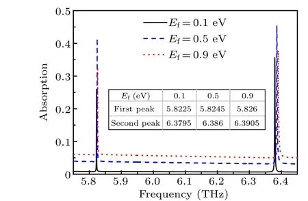
Fig.5. Absorption spectra for different Fermi levels of graphene monolayer.
From Eq.(1), it is found that the surface conductivity of graphene can also be changed by varying the relaxation time.Therefore, the absorption spectrum can be tuned by slightly changing the relaxation time,which is achieved by controlling the carrier mobility in graphene since τ =μEf/ev2f(μ is the carrier mobility and vfis Fermi velocity).The absorption spectra for different values of relaxation time τ are illustrated in Fig.6.It can be seen that the absorption of both resonant peaks increases with τ decreasing. In addition,the background absorption also increases correspondingly. However, the resonant frequencies of both peaks remain almost unchanged.
Typically, the guided mode resonance is sensitive to the variation of incident angle, which correspondingly results in the change of absorption peak. Such a phenomenon can be employed to tune the ultranarrow dual-band absorption properties of the proposed absorber.
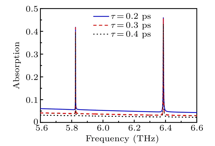
Fig.6. Absorption spectra for different relaxation time τ.
4. Conclusions
In this work, a tunable dual-band terahertz graphene absorber, which consists of a graphene monolayer on a guidedmode resonant filter, is proposed and investigated theoretically. The graphene absorber presents >40% absorption at two resonance frequencies, which is attributed to the guided mode resonances with different mode numbers. The analysis of electric field intensity distributions is utilized to give the underlying physics of such dual-band enhanced absorption effects. In addition, the influence of geometric parameters on the absorption spectrum is studied, which will provide useful guidance for fabricating this absorber. Finally, the optical properties of graphene, including the influences of Fermi level and relaxation time on the absorption spectrum are investigated. We believe that the results can be conducive to realizing the applications in biosensing and detector with high sensitivity.
杂志排行

Chinese Physics B的其它文章
- Two-dimensional finite element mesh generation algorithm for electromagnetic field calculation*
- Stable water droplets on composite structures formed by embedded water into fully hydroxylated β-cristobalite silica*
- Surface active agents stabilize nanodroplets and enhance haze formation*
- Synchronization mechanism of clapping rhythms in mutual interacting individuals*
- Theoretical study of the hyperfine interaction constants,Land´e g-factors,and electric quadrupole moments for the low-lying states of the 61Niq+(q=11,12,14,and 15)ions*
- Ultrafast photoionization of ions and molecules by orthogonally polarized intense laser pulses: Effects of the time delay*