Priori information analysis of optocoupler accelerated degradation experiment based on failure mechanism verification test
2020-05-23XungongZhngXihuiMuJingFengHuizhiLi
Xun-gong Zhng , Xi-hui Mu , Jing Feng , Hui-zhi Li
a Department of Ammunition Engineering, Army Engineering University Shijiazhuang Campus, Shijiazhuang, 050000, China
b Hunan Ginkgo Data Technology Co., Ltd., Luositang Road, Changsha, Hunan, 410100, China
Keywords:Priori information Failure mechanism Failure mechanism verification test Accelerated degradation
ABSTRACT The optocoupler is a weak link in the inertial navigation platform of a kind of guided munitions. It is necessary to use accelerated storage test to verify the storage life of long storage products.Especially for small sample products, it is very important to obtain prior information for the design and implementation of accelerated degradation test. In this paper, the optocoupler failure mechanism verification test is designed and the experimental results are analyzed and the prior information is obtained. The results show that optocouplers have two failure modes, one is sudden failure and the other is degradation failure; the maximum temperature stress of optocoupler can't exceed 140°C; the increase of leakage current of optocoupler is caused by movable ions contaminating the LED chip. The surface leakage current is proportional to the adsorption amount. The increase of leakage current makes p-n junction tunneling effect occur which LEDs the failure of the optocoupler.The lifetime distribution model of the optocoupler is determined by the failure physics. The lifetime of the optocoupler is subject to the lognormal distribution.The degeneracy orbit of the optocoupler leakage current is described by a power law model. The estimated values of the orbital parameters are initially calculated and the parameters of its life distribution function are deduced. The above information lays a good foundation for the optimization design and data processing of the accelerated degradation experiment.
1. Introduction
As a kind of important device of a certain type of guided missile inertial navigation platform, a certain type of optocoupler is responsible for isolating various electrical signals for the inertial navigation platform and avoiding the interference of the electrical signals of various components in the inertial navigation platform.Through the electrical parameter detection of the inertial navigation platform of a certain type of guided munition that has reached the service period and expired service, it is found that the optocoupler is the weak link of the weapon system,and its reliability is less than traditional weak parts such as accelerometers and gyroscopes. Since optocouplers are highly reliable and long-life products,traditional life tests not only consume a lot of manpower and material resources,but also often have long test cycles.Accelerated degradation test is an important technical approach to solve the reliability assessment of high-reliability and long-life products.There are a large number of literatures currently studying accelerated degradation tests (ADT) [1]. At present, the optimization design of accelerated degradation test is divided into two major categories: analytical solution method and simulation-based method. Tseng and Yu put forward a degradation test termination criterion to make the statistical results of the data most accurate[2]. Under the constraint of cost, Wu and Chang aimed at the minimum mean square error of the p-order fractional life,and they established a degradation test optimization design method for the degradation rate obeying the exponential distribution[3].While Yu and Tseng did the same thing with the degradation rate obeying the lognormal distribution and the reciprocal Weibull distribution[4,5]. The above literature all uses analytical methods to optimize the accelerated degradation test.Because the derivation process of the analytical method is very complicated, the simulation-based method is usually used to optimize the design now. Wang and Zhang[6]presented the general flow of the optimization design of accelerating degradation test scheme based on mixed-effects model under the simulation-based method. Pan studied the optimal design of step-down accelerated degradation test under the condition of small sample size using the Monte-Carlo simulation method [1]. Tan studied the optimization scheme of accelerated degradation test based on simulation in the condition of competitive failure [7]. However, the main problem of the simulation method facing is to specify the form of the degenerate orbit model and specify that some coefficients follow the inverse Weibull distribution,which is a big restraint for it.It should be pointed out that whether it is an analytical method or a simulation-based method, the optimization design of accelerated degradation test is inseparable from the priori information. Transcendental information includes degenerate orbit models, accelerated degradation equations and preliminary estimates of correlation coefficients.The literature of various types of research on accelerated degradation test optimization methods often uses the prior information given in other literature, or summed up through historical data [8]. However,the problem is that due to various reasons,the historical data of some products are incomplete or cannot be collected.In this case,a failure mechanism verification test is required to obtain the prior information.In this paper,the optocoupler used in a certain type of guided missile was tested through failure mechanism verification experiment. Based on the determination of its failure mechanism,the test data was analyzed and deduced,and the prior information required for the optimal design of the accelerated degradation test was obtained, which lays a good foundation for optimal design.
This article is divided into five parts, the first part is the introduction, mainly discussing the problem of prior information acquisition for accelerated degradation test and the significance of the study in this paper;the second part is the setting of the failure mechanism verification test program and the description of the test results; the third part is the failure mechanism analysis of the optocoupler and the derivation of the lifetime distribution; the fourth part is the derivation and fitting of the degenerate orbit, as well as the estimation of the relevant estimates;the fifth part is the conclusion.
2. Test scheme design and test data visualization
2.1. Structure introduction and test scheme design
There are two types of optocouplers: one is a nonlinear optocoupler and the other is a linear optocoupler. According to the classification, the optocoupler studied in this paper is a nonlinear optocoupler. More specifically, the optocoupler is a switch-type optocoupler, and its specific structure is shown in Fig.1:
This type of optocoupler is a four-legged photosensitive resistance type of optocoupler. The tube foot is plated gold dust to increase the conductivity of the pin,and the head is coated with black paint to further insulate the external light. Its left is LED and its right is photosensitive resistor.According to the foregoing,this type of optocoupler is used as a solid switch.Its functional test is shown in Fig. 2.
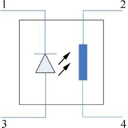
Fig.1. Schematic diagram of optocoupler structure.
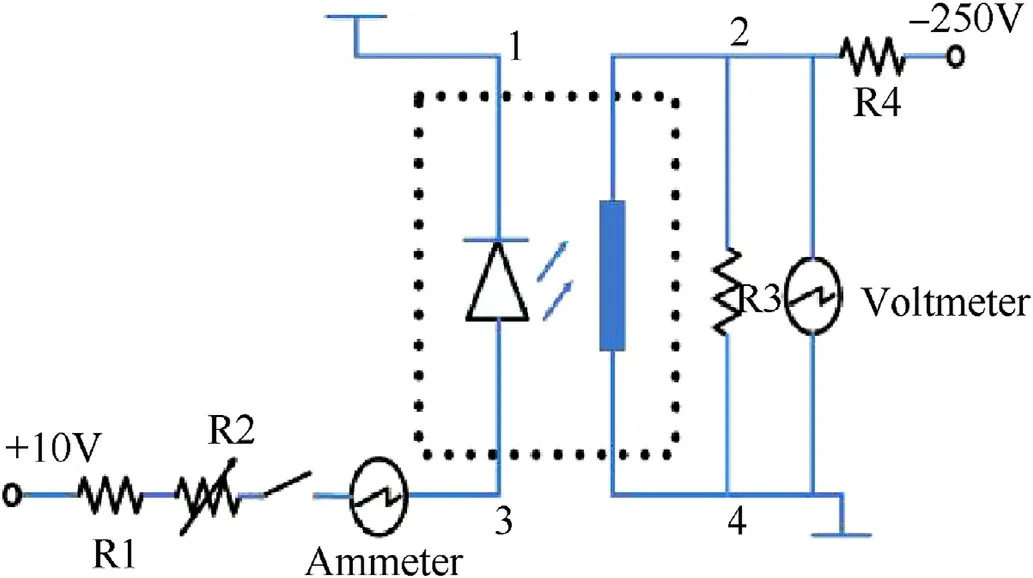
Fig. 2. Schematic diagram of optocoupler functional test.
The test process of Fig. 2 is identical to the operational experience of the optocoupler in the missile. When the right given to -250 V voltage and left without electricity, the photosensitive resistance (that is, the dark resistance) is not less than 10 MΩ,conversion on the voltmeter readings (dark voltage) is not greater than-215.146 V.When the left side is energized and the current is 12 mA, the right voltage is rapidly reduced, and the voltage representation number (that is, the conduction voltage) should not be less than-1.8 V,also known as the flip voltage.It can be seen from Fig. 2 that the optocoupler studied in this paper is only used as a solid-state switch and belongs to a nonlinear optocoupler. Many literatures have studied linear optocouplers. For linear optocouplers, the current transfer ratio (CTR) is a very important parameter, and since the nonlinear optocoupler does not have a CTR parameter, CTR is not selected as a parameter to characterize the optocoupler performance.Therefore,the ordinary optocoupler and the optocoupler studied in this paper are completely different in function. The former is mostly a linear optocoupler, which controls the transmission of current,while the latter is used as a circuit switch.After the previous factory visits and literature research,the test parameters that represent the optocoupler performance are not only dark voltage and flip voltage, but should be five parameters. These five parameters are: dark voltage, flip voltage, LED forward working pressure drop, reverse breakdown voltage and reverse leakage current.The first two parameters correspond to the performance of the photoresistor, and the last three parameters correspond to the performance of the LED.
For the optocoupler inside the missile control system, most of the time is in stock, and the test and transportation time only occupies a small amount of time during the storage period.Therefore,temperature stress and humidity stress are the main environmental factors that affect the reliability of optocoupler storage.For this type of optocoupler,it is a sealed design.All functional parts are packaged in a metal case. The pins are gold-plated to reduce resistivity and resist corrosion.In addition,the optocoupler is placed in an electronic compartment inside the missile control system.The electronic compartment is integrally sealed with polyurethane foam, which can also effectively resist water vapor erosion.Therefore, in theory, moisture is only possible to enter during the optocoupler production process. Therefore, the effect of humidity on the optocoupler is limited. The main consideration is the influence of temperature stress on the storage reliability of the optocoupler.
Therefore,the method of stepping temperature stress is used in the test. Since one of the purposes of this experiment is to determine the ultimate temperature of the optocoupler,the temperature limit is not set.Specific way is as follows:the temperature range is divided into three parts, the first paragraph is from 30°C to 50°C,10°C for step length; The second paragraph as 50°C-100°C, 5°C for step length; The third paragraph from 100°C to test cut-off temperature, with 2°C for step length. At any test temperature point, the test is performed at room temperature. To ensure this,the rules are as follows:in the first stage, the heating time and cooling time are one hour;In the second stage,the heating time is constant and the cooling time becomes two hours. In the third stage, the heating time is constant and the cooling time becomes three hours.
The test scheme section is shown in Fig. 3.
Three temperature points are chosen to be tested three times,50°C, 80°C and 100°C. Other temperature points are tested only once.Because the sample is expensive,but considering that the test parameters may interact with each other,the failure mechanism is not necessarily unique.The sample can neither be too much nor too little,so three samples are used in this test.In addition,the reason for using three samples is that although there is no clear standard and document support, according to engineering experience, the determination of any one distribution requires at least three points.Therefore, three samples were selected as the number of experimental samples.When one of the following conditions occurs,the sample is withdrawn from the test: 1. The functional indicator flipped voltage reaches a given threshold. 2. The data suddenly changes dramatically, the optocoupler will be returned to the last temperature, and then test again after cooling. If the data can be recovered,it will continue to be heated up,and if not,exit the test.
2.2. Test data visualization
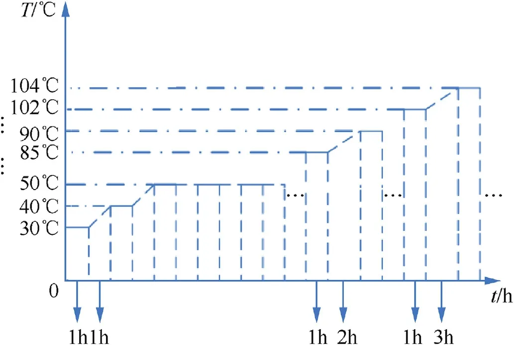
Fig. 3. Test scheme section.
According to the set test plan, the sample was tested. The dark voltage of the photoresistor did not change throughout the test.The flip voltage as an indicator of the optocoupler function and the forward voltage drop characterizing one of the LED performance parameters changed very little.Instead,The two parameters of LED reverse leakage current and reverse breakdown voltage varied greatly. During the experiment, two optocouplers did not degenerate but suddenly failed (145°C and 147°C). After laboratory testing and analysis, it was considered that the internal LED's connecting line was broken and an open circuit caused their failure.Specifically,the junction of the surface of the LED chip is separated from the lead connecting it,resulting in an open circuit.This may be due to defects in the bonding process, or poor quality of the transparent adhesive.
The remaining optocoupler produced significant degradation.So the optocouplers have two failure modes, one is sudden failure and the other is degradation failure. Obviously the two are independent of each other. Fig. 4 and Fig. 5 show the reverse leakage current and breakdown voltage as a function of temperature and time.
As shown in Fig.4,the abscissa represents time,the left ordinate represents temperature, and the right ordinate represents data measured at room temperature after heating at the corresponding temperature for 1 h. The blue step line in the figure indicates the stepping temperature.Red lines and data points indicate the values of the measured parameters. Three hours of heating were performed at 50°C, 80°C, and 100°C respectively. After each hour of heating, the temperature was cooled to room temperature and related parameters were measured again.Therefore,at these three temperatures,the ladder lines are longer than the rest.
In the figures above,the breakdown voltage and reverse leakage current of the LED inside the optocoupler have very obvious degradation phenomenons. It needs to be pointed out that the reverse leakage current at the initial test stage (less than 80°C) is measured in nanoamperes (hundreds of nanoamps), and it is measured in microamperes (microamps to tens of microamperes)in the later period. In Fig. 4, the unit is selected as microamperes.Therefore, the reverse leakage current in the early stage is not obvious on the graph.So thinking that early data can be ignored is inappropriate. It can be seen from the figures that the trend of leakage current and breakdown voltage with temperature and time is generally opposite,and there is an inflection point after the 38th hour. After the 42 nd h heating is finished, the optocoupler cannot reverse the voltage and it cannot complete the intended function,which means complete failure.In comparison,the forward voltage drop of the LED in the optocoupler does not change significantly,but there is a phenomenon of slow decline. Therefore, it can be determined that the failure of the optocoupler is caused by the leakage current of the LED and the change in the breakdown voltage. In fact, after the 36th hour of heating is over, the performance of the optocoupler goes into an unstable state. The corresponding temperature is 143°C. Therefore, considering the failure of three optocouplers the maximum temperature stress of the optocoupler cannot exceed 140°C. Since the three samples are all due to failure of the internal LED, the life of the optocoupler is equivalent to the lifetime of the internal LED.
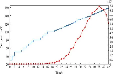
Fig. 4. Leak current line chart with the change of temperature and time.
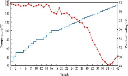
Fig. 5. Breakdown voltage line chart with the change of temperature and time.
3. Analysis of the failure mechanism of optocoupler and its determination of the life model
3.1. Qualitative explanation of failure mechanism
In general, it is assumed that the degradation is generally monotonic, but the leakage current and the breakdown voltage caused an inflection point after heating in the 38th hour.The causes of LED reverse leakage are more complicated and varied, specifically,including production process defects,chip defects,and static problems. Process defects are mostly caused by excessive silver glue, chip cracking and solder ball offset or excessive solder balls.Chip defects are mostly caused by movable ion contamination and p-n junction collapse.Static problems are often caused by induction or friction.In general,the increase in LED leakage current caused by excessive silver glue,solder ball offset or excessive solder ball often occurs during the factory inspection period after the product is packaged, and is found at the beginning. The situation of the chip cracking is different,and it is difficult to be found at the beginning.After the chip breaks, the silver glue slowly penetrates into the surface of the chip along the gap capillary,causing the p-n junction to be short-circuited. However, the cause of this failure cannot explain why the leakage current increases first and then decreases,as does the p-n junction collapse.The same is true for electrostatic problems. The accumulation of static electricity generated by friction or induction is often generated during the production phase.However, in general, static electricity does not easily accumulate high voltage. Although the static electricity condition is random and ubiquitous, it is not always able to release enough energy to cause damage.Damage caused by static electricity is infrequent and is a small probability event. So basically this reason can also be ruled out. The above is the reason for determining the leakage current of the sample LED by the exclusion method, that is, the mobile ion pollution.
According to Xu and Xiao,with the increase of temperature,the first increase and then decrease of the leakage current are the typical active characteristics of mobile ion pollution on the chip and the formation of surface leakage channels in addition [9,10]. The change in leakage current is caused by the contamination of the movable ions on the chip, forming a surface leakage path, which explains why the breakdown voltage exhibits a roughly opposite change with the leakage current. One of the reasons is that the existence of the surface leakage channel is equivalent to the parallel connection of a resistor, which will cause the overall resistance of the p-n junction to decrease, which in turn causes the reverse breakdown voltage to decrease. Therefore, the increase of the leakage current is the cause of the breakdown voltage drop.Another reason will be explained in the section of determining the life distribution model.However,the current literature is not clear for further explanation on how to form a surface leakage channel.By studying related literature, this problem can be explained from two perspectives:quantum physics and surface chemistry.
3.1.1. Quantum physics aspect
It is generally believed that the composition of LED reverse leakage current consists of the following two currents:the current of the tunnel through the barrier the hot electron emission current over the barrier [11].In the case of not very high temperature,the tunnel current is the main one,and the thermal electron emission current is very small and can be ignored.
In the production of LED chips,due to the complete periodicity of the crystal lattice, the surface state is generated by the sudden interruption of the crystal surface.The atoms on the semiconductor surface have only one side with adjacent atoms. On the vacuum side, the valence electron does not have covalent bond with it.Therefore,each surface atom has an unpaired electron,which is in a localized orbit that points away from the surface.This kind of track is often referred to as a “suspended bond”.These suspended bonds adsorb certain positive ions (such as Na+, Cu+, etc.) [23], When these impurity ions“congregate”on the surface of the p-n junction and its vicinity, a leakage path traverses across the p-n junction surface [12]. When add reverse voltage, voltage is applied to not only for the inside of the semiconductor,but also at the same time will be applied to the surface of the semiconductor, forming a surface recombination current or surface leakage current, which results in increased reverse leakage current.
On the other hand,according to Roderick's research,on the edge of the contact between metal and semiconductor, the effect of tunnel effect is especially obvious due to the decrease of the width of the barrier and the decrease of the image force because of the concentration of power lines and the increase of electric field intensity [13].The effect is even more pronounced if the surface of a semiconductor near a metal surface accumulates a positive surface charge that makes the barrier thinner. The effect is even more pronounced if the surface of a semiconductor near a metal surface accumulates a positive surface charge that makes the barrier thinner. The effect is even more pronounced if the surface of a semiconductor near a metal surface accumulates a positive surface charge that makes the barrier thinner. Therefore, due to positive ions, the current of the tunnel will become larger, which will increase the overall leakage current.
3.1.2. Surface chemistry aspect
As is mentioned,the surface of the chip,due to the existence of a“suspended bond”, will adsorb some positively charged ions.Adsorption is the phenomenon that atoms, molecules, or ions of a substance are attached to the surface of another substance.Adsorption is divided into physical adsorption and chemical adsorption. According to Langmuir adsorption theory, the adsorption of some positively charged ions on the semiconductor surface belongs to chemical adsorption [14]. In the chemical adsorption,adsorbents and adsorbents combine in the form of chemical bonds to approximate chemical reactions, and thus require certain activation energy [15]. Therefore, chemical adsorption usually takes place at a certain temperature, and in a certain range, the adsorption speed is accelerated with the increase of temperature. Unlike physical adsorption,chemical adsorption is basically carried out on monolayer on the surface of adsorbent and has saturability. At the same time,due to the influence of thermal motion,the desorption reaction is also carried out, namely, ions leave the semiconductor surface. So both reactions go together, also called the “confrontation reaction”[16].Since the adsorption reaction is the exothermic reaction, when the temperature is further increased, it will not be conducive to the adsorption. When the reaction rate of the desorption is greater than the adsorption rate,the total adsorption capacity of the moving ions on the semiconductor surface will decrease,and the leakage current will be reduced by combining the previous quantum physical interpretation.
Based on the above analysis,the increase of the leakage current of the optocoupler is due to the formation of surface leakage channels which is due to the contaminated movable ions on the chip. As mentioned above, the leakage current and breakdown voltage of the sample are generally opposite, and the inflection point is also the same.After calculating the correlation coefficient of the two,it is 0.9867.It can be seen from the correlation coefficient that the correlation between the leakage current of the optocoupler and the breakdown voltage is very close to 1,which can correspond to the previous physical interpretation, thus forming a surface electric field or surface composite current.
3.2. Mathematical relations of surface current and surface complex quantity
The foregoing qualitatively explained that as the adsorption area increases or decreases, the surface current increases or decreases.The relationship between surface current and surface adsorption complex amount is deduced by the surface resistance formula below.
As shown in Fig.6,suppose that the surface recombination area isA,the length parallel to the current direction isL,the thickness of the ion layer isD,and the width of the surface compound amount isl, then the ion source bottom areaSis:

According to the surface resistance formula [17], there are:

Then:
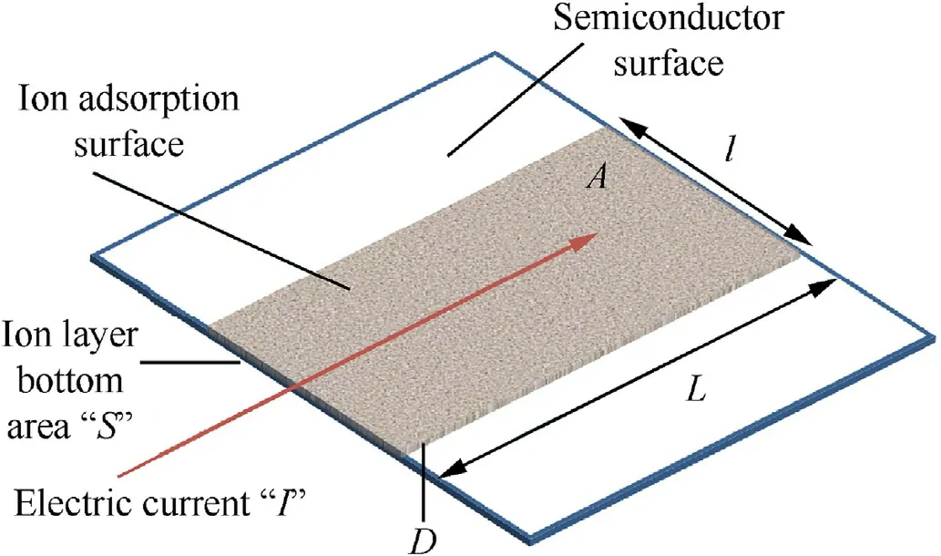
Fig. 6. Ion adsorption schematic diagram.

According to Ohm's law, the surface composite current I is:

Surface composite area A satisfies:

And then,

Then the expression formula of I becomes:

In the above equation,Lis a fixed value.Assuming only one kind of ion adsorption, then ρ is a fixed value. As mentioned above,chemical adsorption is basically carried out on monolayers of the surface of the adsorbent. In other words, the thickness of the adsorbed ion layer is determined by the ions themselves.Assuming that only one kind of ion is adsorbed,Dis also a fixed value. In addition,since the reverse voltageUapplied each time is fixed,and the surface resistance caused by adsorption is in parallel with the impedance inside the semiconductor, and does not involve a voltage division problem,Uin the above equation is also constant.Assuming the tunnel current is negligible (several nanoamps to several tens of nanoamps),Iis proportional to adsorption areaA,thus:

Ais the surface adsorption area.According to the surface chemical interpretation above, it is actually the amount of adsorption.Therefore,the surface leakage current is in direct proportion to the amount of adsorption, and the reverse leakage current curve can fully represent the curve of adsorption amount.
3.3. Determination of optocoupler life distribution model based on failure physics
In Sections A and B,the causes of changes in leakage current and breakdown voltage are given by analysis.The breakdown voltage is reduced due to the increase of leakage current,and the increase of leakage current is due to the formation of surface leakage channels due to movable ion contamination, and the physical and chemical explanations of the increase of leakage current and the quantitative relationship between the surface and the composite amount are given. As mentioned above,one reason for the drop in breakdown voltage is that the presence of a surface leakage path is equivalent to a resistor connected in parallel, which causes a decrease in the overall resistance of the p-n junction, which in turn causes a decrease in the reverse breakdown voltage. However, the parallel resistance formed is not the essential cause of the deterioration of the p-n junction performance of the LED, but the performance of the p-n junction is degraded due to the presence of the surface leakage channel changing the surface state of the p-n junction[18].This is another reason for the breakdown voltage drop.
According to the semiconductor p-n junction tunnel breakdown theory,the tunneling probability of a microparticle with a mass of μ and with energy E of crossing the barrieru(x)is:

If the tunnel length is short,or the barrier heightu(x)-E is low,the tunneling probability will increase, which causes the carrier concentration in the cut-off layer to increase to form a large tunneling current under the applied electric field. As mentioned above,if a positive surface charge accumulates on the surface of the semiconductor near the metal, the barrier at the edge is made thinner, and the tunneling effect is more pronounced. In addition,Xue[19]pointed out that when the “dangling bond”on the surface of the p-n junction adsorbs ions,defects are formed.These defects will form local quantum states around them,and the corresponding energy levels will be within the forbidden band,causing the deeplevel defect density to become larger [20]. The region where the deep-level defect density is larger has a larger tunneling probability of the electron crossing barrieru(x),so that the reverse breakdown voltage is low.The reverse breakdown voltage will affect the carrier transport process when the LED is working in the forward direction[21],which will further darken or flash the LED when it is working,which makes the optocoupler voltage flipping difficult. Therefore,the essential cause of LED failure inside the optocoupler is that tunnel breakdown occurs,and the tunnel breakdown occurs due to the leakage path formed on the surface of the p-n junction.
Gao [22] obtained the log-normal distribution of the p-n junction under the premise that the p-n junction tunnel breakdown caused the failure,so no further derivation is made here.Therefore,based on the above analysis,the life of the LED can be determined,that is, the life of the optocoupler is also subject to a lognormal distribution from the perspective of p-n junction tunnel breakdown.Therefore,based on the above analysis,the life of the LED can be determined,that is,the life of the optocoupler is also subject to a lognormal distribution from the perspective of p-n junction tunnel breakdown. Since two samples in this test produced sudden failures and the sample size was too small, it was impossible to determine the distribution pattern of the optocoupler life in the case of sudden failure. From the perspective of accelerated test design,it is only possible to consider the degradation process first,and then consider the case of sudden failure. Therefore, the life distribution is initially determined to be a lognormal distribution,and the regression model is fitted and the relevant estimates are obtained. This is always better than blindly performing a formal accelerated degradation test on the optocoupler.
4. Determination of degradation models and preliminary estimation of related parameters
4.1. Determination of degradation models
When the deterioration of a product's performance degradation characteristics or product health status can be characterized by a key performance parameter, failure performance modeling,degradation distribution modeling, generalized degenerate modeling,stochastic process degradation modeling,Gauss-Poisson model, and degradation modeling with change point can be considered to establish a performance degradation model,and then product reliability analysis can be implemented [23]. Since the failure mechanism of the degradation of the optocoupler has been analyzed in detail through the analysis of the verification test, the degradation physics model of the leakage current is used to establish the degradation model. The so-called failure physics model refers to the corresponding degenerative orbital model established by analyzing the changing laws of the physical or chemical mechanisms that cause product failures,and the internal relations between product failures and the conditions of use(environmental stresses). Typical failure physics models include cumulative damage models, chemical reaction theory models, and models based on degradation rates. The model describing the internal damage accumulation process of materials is called cumulative damage model.Common cumulative damage models include Paris model, power law model and Birnbaum-Saunders model(abbreviated as BS model)[24].The basic idea of the reaction theory model is that the damage and degradation of materials and components are generally caused by physical-chemical processes such as corrosion,wear,and diffusion.When these processes continue to a certain degree,the failure will occur.The model derived from the modeling of degraded orbits by means of physical-chemical processes is called a reaction theory model.In essence,what it shows is the continuous accumulation of damage[25].The model based on the degradation rate differs from the previous two models.Both of the above models directly obtain the degradation track of product performance by analyzing the product failure mechanism. The model first establishes the degradation rate model, and then uses the integral method to obtain degenerate orbits.
In summary,it can be seen that because the failure mechanism of the product is already known, it is more appropriate to use the cumulative damage model or the reaction model than to use the model based on the degradation rate.
From an intuitive perspective,according to the modeling theory of the reaction theory model, the degeneracy model of the optocoupler leakage current is the most suitable for the reaction theory model.The reaction theory model is given by foreign scholars when studying the failure of circuit boards due to the growth of fine fibers between insulating materials [26]. The basic assumption is: Let materialA1undergo a chemical reaction toA2under certain environmental conditions (such as temperature, humidity, electricity,etc.) as follows:

Wherekis the reaction rate constant and the reaction is expressed as:

Solving the above two differential equations, we can get the relationship betweenA2and timet(includingA1(0) andA2(0)).However, the above differential equations are derived from the reaction (I). According to the theory of reaction kinetics, the reaction is a first-order reaction, and the differential equations of second-order reaction and the above become very complicated.The first-order reaction requires that only one kind of material reacts,or when the two materials react,the measurement coefficient and the initial concentration are equal, or when more than one kind of material reacts, all the substances other thanAare in excess (the amount exceedingAis at least 10 times) [27].The fine-conducting fibers studied by foreign scholars are composed of cupric chloride.Compared to chlorine,the amount of copper is almost infinite,and it is far more than the amount of chlorine.Therefore,a degenerate model can be constructed through a reaction theory model.For the optocoupler leakage current parameters, due to the opposing reaction is already very obvious in the late period,obviously neither the semiconductor surface nor the ionic impurities can produce an overwhelming advantage to the other party in terms of quantity.On the other hand, it is assumed that a “chemical reaction” occurs between the surface of the semiconductor and the ionic impurities,but the quantitation coefficient and the starting concentration cannot be guaranteed to be equal.Therefore,in theory,the reaction theory model is not suitable for the degradation modeling of the product.
Based on the experimental data, a reaction model was fitted preliminarily.The leakage current values at 50°C,80°C,and 100°C are used here.There are three values at each temperature.Through matlab fitting,it was found that its decision coefficientR-square is less than 0.1. This shows that the reaction theory model is not supported from the perspective of data.
From the previous analysis, we can see from the perspective of physical modeling of failure, the reaction model is not suitable.Consider the cumulative damage model. As mentioned earlier, it usually has three forms: Paris model, power law model and BS model.The Paris model is often used for mechanical failure caused by the expansion of metal fatigue cracks.The BS model is often used for failure due to cyclic loading.The power law degradation model is often used for modeling of degradation such as resistance degradation,cable aging,and concrete corrosion[28].Theoretically speaking,the former two types are not suitable for the modeling of leakage current degradation of optocouplers.Therefore,the use of a power law degradation model to construct a degradation model of leakage current is considered. The power law model describes the relationship between the degradation amount and the generalized time [29]. Assume that the performance parameters of a product change monotonically with the extension of working hours,and the performance parameters at time t satisfy:

Wherey(t)is the degenerate quantity;β1and β2are the degenerate model parameters, β1is the degeneration rate factor, which is related to the working environment stress, β2is the shape parameter of the degeneracy curve, and only related to the manufacturing material of the product, t is the generalized time.
Since the leakage current of the optocoupler is already present at the factory, the power law model is modified to add an initial valueC. Due to the uncertainty of production assembly, the initial value of leakage currentCcan be regarded as normal distribution,thusFor the sake of simplicity,Cis taken as a constant here. Therefore,the power law model can be rewritten as:

Using matlab to fit data of 50°C, 80°C, and 100°C. There are three values at each temperature. The fitting results are shown in the following table:
As can be seen from Table 1,when using the modified power law model to fit the data, from theR-square, the fitting effect is very good.The reason why the value ofCchanges greatly is because the data used is the amount of degradation of the leakage current of the same optocoupler at different temperatures. The data represented by theCvalue means the amount of deterioration of the leakage current before 50°C, before 80°C, and before 100°C. According to the comparison with the actual value,the error of the fittedCvalue does not exceed 0.8%.β2as the shape parameter of the degeneracy curve should itself be fixed.It can be seen from Table 1 that β2floats up and down around 2.Its mean value is 2.141.β1is a degradationrate factor and is related to environmental stress.

Table 1 Regression model parameters fitting results.
For degraded products, according to the definition of degradation failure, when the performance reaches the failure threshold with time, the product is considered to be ineffective, and the corresponding time is the life of the product [30]. For the optocoupler,if the leakage current at timetisy(t),the failure threshold isD. When the leakage current reaches the failure threshold with time, the optocoupler fails, and the lifetime of the optocoupler is the first time that the leakage current reaches the failure threshold:

Taking into account the storage conditions, the leakage current is monotonically increasing with time, and the lifetime of the optocoupler can be obtained from the following equation:

The lifetime of the optocoupler follows a lognormal distribution,thus

Further,

In the above formula,(D-C)and β2are constants,therefore,β1is obeying a lognormal distribution,and is denoted asμβand σβrepresent the logarithmic means and logarithmic standard deviation of the degradation rate distribution respectively.
In summary, the degeneration trace of the optocoupler leakage current can be described by the hybrid effect model as follows:

(i) In the above equation, β1andCare random, which respectively reflect the differences of the initial values and the degradation rates of different optocouplers. For simplicity,considerCas a constant. β2is a fixed constant for the adsorption and leakage mechanisms.
(ii) Leakage current degradation rat β1meets the Arrhenius equation. Its logarithmic standard deviation σβhas nothing to do with the level of accelerated stress,that is,σβdoes not change with temperature. The relationship between the logarithm mean μβof β1and temperature T (°C) satisfies:

Where α1and α2are model parameters of acceleration equation.Through the β1value obtained from the previous fitting,the values of α1and α2can be estimated by the least squares method,and the linear unbiased estimation of σβcan be performed. The specific results are shown in Table 2.
4.2. Optocoupler lifetime distribution model parameters
The optocoupler degradation failure model is:

Table 2 Relevant estimates table.

As mentioned earlier,for the sake of simplicity,assuming thatCis a constant, the degenerate failure model of the optocoupler can be deduced from the definition of degradation failure:
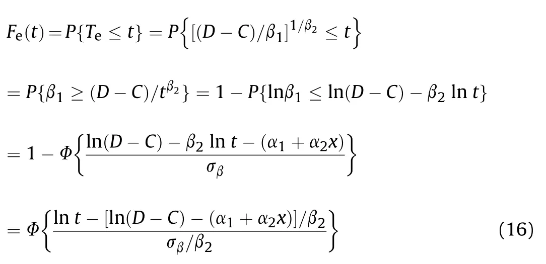
In the above formula, φ{·} is a standard normal distribution function. Let:

Then the above equation can be simplified as:

In this way,the lifetime distribution model of optocoupler under degradation is deduced. From the above equation, the lifetime is obeying the lognormal distribution,and the logarithmic mean and logarithmic standard deviation are respectively μeand σe.
5. Conclusion
In this paper, through the data analysis of the optocoupler failure mechanism verification test, the prior information of the optocoupler life assessment is obtained. The conclusions are as follows:
(1) The optocouplers have two independent failure modes, one is sudden failure and the other is degradation failure.
(2) The maximum temperature stress of the optocoupler cannot exceed 140°C; the increase of the leakage current of the optocoupler is due to the formation of surface leakage channels which is due to the contaminated movable ions on the chip, and the surface leakage current is in direct proportion to the amount of adsorption;the increase of leakage current causes the tunneling effect of the internal p-n junction of the LED,which in turn affects the performance of the LED and causes it to fail.
(3) The degeneration trace of the optocoupler leakage current can be described by the hybrid effect model as follows:
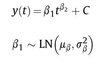
In the above equation, β1is random, β2andCare a fixed constant for the adsorption and leakage mechanisms.Leakage current degradation rate β1meets the Arrhenius equation. Its logarithmic standard deviation σβdoes not change with temperature. The relationship between the logarithm mean μβof β1and temperature T (°C) satisfies:

(4) The storage life of the optocoupler follows a lognormal distribution. Its lifetime distribution model is:

Where μe= [ln(D-C)- (α1+ α2x)]/β2and σe= σβ/β2.
(5) The preliminary estimate of each parameter is:
The determination of the failure mechanism helps clarify the upper temperature limit and temperature selection during the formal test, avoiding over-temperature and failure mechanism changes. The determination of degenerate trajectories and life distribution models and the estimation of various parameters are the basis for selecting the optimal design for accelerating degradation tests.It is also possible to avoid the misadjustment of the life model in the later experimental data processing. The above priori information lays a good foundation for both the accelerated degradation test design of the next step and the formal acceleration degradation test.
This work is supported by the National Natural Science Foundation of China of China (No.61471385).
杂志排行
Defence Technology的其它文章
- A comparison of the ballistic behaviour of conventionally sintered and additively manufactured alumina
- Effect of operating temperature on aged single lap bonded joints
- Investigation on energy output structure of explosives near-ground explosion
- Characteristics structure analysis on debris cloud in the hypervelocity impact of disk projectile on thin plate
- A fast-running method for blast load prediction shielding by a protective barrier
- Coating processes towards selective laser sintering of energetic material composites
