Nano-sphere surface arrays based on GaAs solar cells
2020-01-15YinshengPengShufengGongKaiLiuandMinghaiYao
Yinsheng Peng, Shufeng Gong, Kai Liu, and Minghai Yao
College of Information Engineering, Zhejiang University of Technology, Hangzhou 310023, China
Abstract: In this paper, we present our efforts on simulating and analyzing the effect of two-dimensional nano-sphere surface array on the characteristic of GaAs solar cells. Based on the scattering and diffraction theory of the photonic crystals, the simulation results show that the distance of adjacent nano-spheres (D) has the pronounced influence on the conversion efficiency and exhibits much poor tolerance, the absolutely conversion efficiency is reduced by exceeding of 2% as the D varies from 0 to 1 μm, in addition, the lower conversion efficiency (< 18%) is exhibited and almost remains unaltered when the D is of > 2 μm.The radius (R) of nano-spheres demonstrates much great tolerance. For D = 0, the solar cells exhibit high conversion efficiency(> 20%) and the efficiency is only varied by less than 1% when R is varied in a very wide region of 0.3-1.2 μm. One can also find out that there is good tolerance for efficiency around the optimal value of refractive index and there is only about 0.2%decrease in final cell efficiency for around ±24% variation in the optimal values, which implys that it does not demand high precision processing equipment and the whole nano-sphere array could be fully complemented using self-assembled chemical methods.
Key words: GaAs solar cell; nano-sphere array; reflection; absorption; conversion efficiency
1. Introduction
The GaAs semiconductor material has been known as one kind of important optoelectronic materials that provides direct band gap energy and high mobility carrier properties.Therefore, the material is commonly used to fabricate high conversion efficiency solar cells and have also been attracted much attention in recent years because of their high conversion efficiency compared to the other solar cells[1-3].
It is well known that surface texturing can be utilized to improve the conversion efficiency of the solar cells. By introducing surface texture, it results in the reduced reflection losses,enhanced light scattering and diffraction of light in the solar cells. Recently, the surface texturing technique has widely been utilized in the fabrication of silicon based solar cells with various designs such as honeycomb, pyramid, invert-pyramid, and V-trench structures[4-9]. However, the methods mentioned above can be not applied to improve the efficiency of GaAs solar cells. On one hand, since its crystallographic plane is on the <001> surface, there is no convenient etching methods, and unlike for silicon, the surface pyramidal structures can be spontaneously produce. On the other hand, though GaAs solar cells with a micro-hole photonic crystal surface texture by etching processes have been reported to have an increase of conversion efficiency[10], the process and starting materials are not economically viable for scale-up production. In addition, the periodic array is lithographically defined, which further increases the production cost. Moreover, for GaAs solar cells the surface recombination velocity is too high and it is difficult to achieve a good surface passivation.
In general, the antireflection coatings with single, double and triple layers at the top have been used for light trapping in the GaAs solar cells[11]. However, practically till date due to the shortcomings such as fabrication issues and finding suitable materials as the middle layer with desirable refractive indices[12,13], it could not obtain even half of the value suggested in Refs. [14, 15]. Due to these reasons, several new light trapping structures have been proposed, ranging from using randomly roughened surfaces[16]to plasmatic metallic structures[17]. And recently, researchers have also explored for novel structural schemes such as photonic crystals dielectric designs[18,19]. Although the light absorption enhancement could be achieved over broad spectrum using these light trapping structures in theory, these structures are difficult to be engineered, rescale and reproduce. Therefore, it is still a challenge to obtain a surface texturing structure with simple, convenient fabrication and low reflection on the frontal surface of GaAs based solar cells.
This motivated us to concentrate our work on studying surface texturing atop of GaAs solar cells. We found that an alternative solution is to deposit a nano-sphere array with periodic structure using different material by self-assembly method on the surface of GaAs, the light path length can be significantly increased based on the scatting of the nano-spheres and the diffraction of photonic crystals. It should be note that the self-assembly is one of the simplest methods building a two-dimension periodic structure. Furthermore, the light trapping structure has the advantage that the geometrical parameters could be easily varied and the whole structure are easily to be engineered, rescale and reproduce, which is also one of the key motivation for this work. To date, singlejunction GaAs solar cells with a self-assembly micro-sphere arrays deposited on the front surface of GaAs solar cells, microsphere diameter of 1 μm and the refractive index of 1.59,have been reported to have an relatively increased conversion efficiency of 25% experimentally[20]. Thus, further theoretical studies systematically on influence of the nano-spheres surface array on characteristics of GaAs solar cells are still needed to improve the performance of the III-V compound solar cells.

Fig. 1. (Color online) (a) Schematic of the GaAs solar cell with nano-sphere array in side view. (b) Schematic top view of the nano-sphere surface array.
In this work, we present our efforts on simulating and analyzing the effect of two-dimensional nano-sphere surface array on the characteristic of GaAs solar cells based on the scattering and diffraction theory of the nano-spheres photonic crystals[21-25]. The material, the size and the distribution of nano-sphere are the critical parameters limiting the conversion efficiency of solar cells. The results show that the distance of adjacent nano-spheres (D) has the great influence on the conversion efficiency and exhibits poor tolerance, the absolutely reduced conversion efficiency by exceeding of 2%as the D varies from 0 to 1 μm, yet the lower conversion efficiency (< 18%) is observed and almost remains unaltered when the D is of > 2 μm. The radius (R) of nano-spheres demonstrates much great tolerance. For D = 0, the solar cells exhibit much high conversion efficiency (> 20%) and the efficiency is only varied by less than 1% within a very wide R variation region from 0.3 to 1.2 μm. One can also find out that there is good tolerance for efficiency around the optimized value of refractive index (n) and there is only about 0.2% decrease in final cell efficiency, for around ±24% variation in the optimal values, which implying that it does not demand high precision processing equipment and the whole nano-sphere array could be fully engineered using self-assembled chemical methods.
2. Solar cell structure
The proposed surface nano-sphere light trapping structure based on thin film GaAs solar cells has been shown schematically in Fig. 1. The structure consists of a nano-sphere surface coating layer, an Al0.8GaAs window layer, and active layer of GaAs is placed below this window layer. An Al0.35GaAs back window layer is placed below the active layer followed by the Al back reflector. Top contact electrodes are also employed as Fig. 1. The wavelength dependent material parameters are considered for GaAs and AlGaAs[26]and Al[27].
The active material layer has been kept fixed at a particular thickness (here including a 0.5 μm p-GaAs emitter layer,3 μm n-GaAs base and 350 μm GaAs substrate layer). The front and back window layer of Al0.85GaAs and Al0.35GaAs has been set to 0.03 and 0.01 μm, respectively, as thicker window layer might degrade the performance of the device[28].The thickness of the planar metallic Al BR has been fixed to 0.08 μm.
The nano-sphere array at the top is assumed to be a twodimensional hexagonal lattice arrangement, as it would provide better diffraction as compared to the square array. As mentioned previously, the condition is similar to the diffraction grating, the role of the nano-spheres array is to deflect the normally incident light to the oblique direction and the diffracted waves propagates at nearly grazing angle within the solar cells, thus improves light propagate paths within the absorption layer. Thin AlGaAs window layers with higher band gap and heavily doped serve an important role to deflect minority carriers away from the contacts in order to reduce surface recombination[29,30]. The structure shown in Fig. 1 has one nano-sphere array where R represents its radius, and the distance between the two adjacent nano-spheres is indicated by D.
In our article, the optical performance of the solar cell has been analyzed through calculating absorption in the active area and reflection from the top surface through power conversion efficiency and I-V curve simulations. The optical absorption in the solar cells is calculated using the scattering matrix method[31,32]. In the scattering matrix method, the structure is divided into a number of vertically uniform layers that can be periodic in the lateral direction. The electromagnetic field in each layer is represented by an infinite set of plane waves. The method rigorously solves the Maxwell equations by imposing matching conditions for the tangential field components at each layer boundary. The total absorption (A(λ))of the structure is obtained by subtracting the reflection(R(λ)) and the transmission (T(λ)) from the total incident power.
The calculated total absorption in GaAs layer is weighted by the air mass (AM) 1.5 solar spectrum and integrated from 400 nm (λmin) to 900 nm (λmax) to obtain the average absorption

And short-circuit current density,


Fig. 2. (Color online) The conversion efficiency as a function of radius for different D value.
where e is the electron charge, h is Planck constant, c is the light speed in vacuum, andis the incident solar radiation intensity per unit wavelength[33]. The solar cell efficiency can be calculated by

where VOCis the open-circuit voltage, Γfis the fill factor, and Pin=0.1W/cm2is the incident solar power (AM1.5 solar spectrum). The open-circuit voltagewhere k is Boltzmann’s constant, T is the absolute temperature (assumed 300 K), andis the reverse bias saturation current.
3. Results and discussion
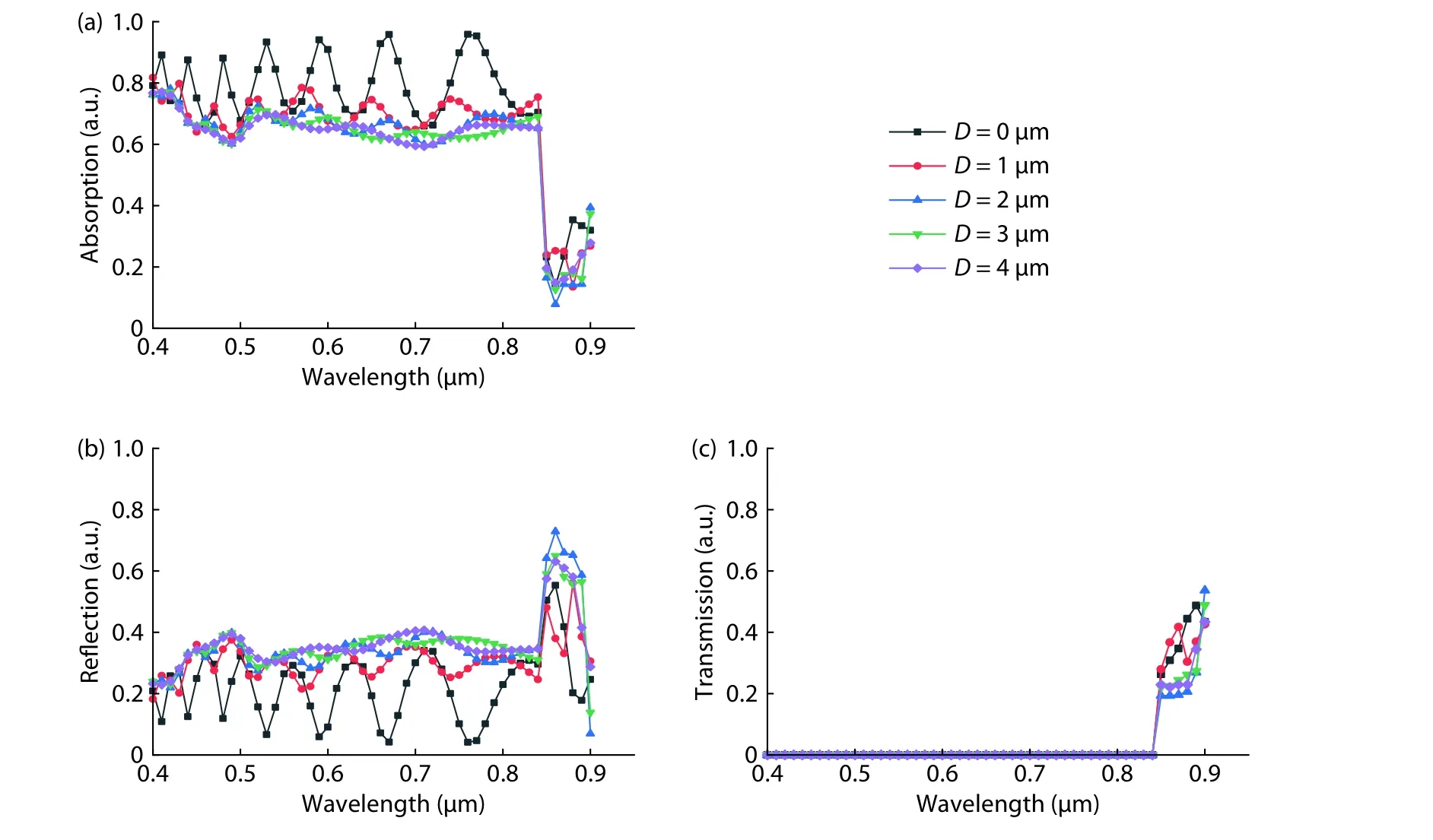
It must be noted that the nano-sphere coating have to be a monolayer to avoid the effects of the photonic crystalline band gap which would interfere with the absorption of the solar cell[34]. To start with, we investigate the influences of the nano-sphere distribution by adjusting the distance of adjacent nano-spheres (D) (as shown in Fig. 1) on the characteristics of GaAs solar cells keeping the nano-sphere refractive index constant of n = 2.0. The overall cell conversion efficiency is calculated as a function of nano-sphere radius (R),and the results with different D value are shown for comparison, as shown in Fig. 2. It was found that the conversion efficiency of solar cells is strongly dependent upon the D value. The results show an increase in conversion efficiency(η)with the decrease of D. Especially the rapid enhancement of conversion efficiency is exhibited when the D decreases from 1 to 0 μm, the maximum efficiency varies from 18.5% to 20.82% with R of 0.6 μm. The absolute efficiency (η)and relative efficiency ( Δη/η) increase are 2.32% and 12.54%,respectively. The conversion efficiency increasing could be mainly contributed from reduced surface reflection losses resulting in light absorption enhancement of GaAs active layer. Fig. 3 demonstrates the spectral graph of absorption,reflection and transmission as function of wavelength in the D variation range of 0-4 μm, respectively. It is found that in the wavelength range of 0.4-0.85 μm the solar cells with D of 0 μm exhibit very low reflection (average value < 20%),significant absorption enhancement (average value > 80%)and almost zero transmission. However, the conversion efficiency exhibits slight variation in the entire absorption wavelength range and has lower value (below 18%) when D is of > 1 μm, as seen in Fig. 2, which is contributed from high surface reflection.
In addition, a series of diffraction peaks are observed,which due to diffraction resonances generated from the electromagnetic waves internally reflected at the surfaces of the wafer when the phase difference between modes reflected from the front and rear surfaces are multiples ofor=mπ/ta, where tais thickness of active layer,represents the photon momentum and m represents a particular mode. The wavelength of diffracted resonant mode is given by[35,36]:

For a triangular lattice, reciprocal lattice vector G has components of Gx=(2π/a)i andrespectively, where i and j are integers. The diffraction resonances occur for integer values of i, j and m and exhibit diffraction peaks as clearly shown in the Fig. 3.
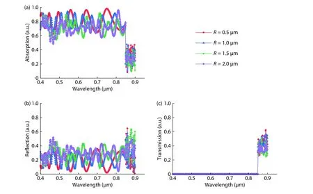
Next, taken the influence of nano-sphere size on the performance of solar cells, Fig. 2 shows that the significant high conversion efficiency (> 20.6%) is observed in the nanosphere radius variation range from 0.3 to 1.2 μm, keeping the distance of adjacent nano-sphere (D) of 0 μm. In addition, for the optimal D of 0 μm, it is found that the conversion efficiency started to rapidly increase and nearly varies linearly from 16.4% to 20.8% when the radius increases from 0 to 0.5 μm. However, the conversion efficiency exhibits very slight variation (around 0.2%) in the wide radius range of 0.5-1.2 μm, then the conversion efficiency started to dip exponentially as the radius of > 1.2 μm and drops below 18%when the radius is of > 2.2 μm. Fig. 4 shows the contour map for photon absorption between radius and wavelength with D of 0 μm. The dense absorption peaks are observed when the nano-sphere radius varies from 0.3 to 1.2 μm in the wavelength range of 0.4-0.85 μm, resulting in enhancement absorption and high conversion efficiency. However, when the radius of the nano-sphere is greater than 1.5 μm or less than 0.3 μm, the absorption peaks significantly becomes sparse, thus resulting in low conversion efficiency. The could be further confirmed by the absorption, reflection and transmission spectra of solar cells, as seen in Fig. 5. From the figure, it is found that the absorption enhancement with the reduction of nano-sphere radius (seen in Fig. 5(a)), which is mainly responsible for reducing of reflection on the surface of solar cells (seen in Fig. 5(b)) and the much low transmission in the wavelength ranges of 0.4-0.85 μm, as shown in Fig. 5(c).

Fig. 3. (Color online) Calculated spectral distribution graph for (a) absorption, (b) reflection and (c) transmission for different D values with n = 2 and R = 0.6 μm.

Fig. 4. (Color online) Shows the contour map for photon absorption between radius and wavelength with D of 0 μm.
It is interested to find that the extremely weak photon absorption is observed in long wavelength range of 0.85-0.9 μm regardless of nano-sphere R and D, as shown in Fig. 3(a) and Fig. 5(a). This is due to the enhancement of reflection and transmission from the solar cells in the long wavelength range. The significant diffraction resonance occur is required that the photonic crystal period (indicated by a as shown in Fig. 1, a =D+2R) is larger than wavelength of light in the active layer (λ/n(λ)), i.e., a >λ/n(λ), where n(λ)represents the refractive index of active material at that particular wavelength[27]. For D < 2 μm, corresponding to smaller period, solar cells exhibit weak diffraction resonance resulting in high surface reflection in the long wavelength range of 0.85-0.9 μm, and the maximum reflection reaches 60%.However, when D increases, correspondingly period increases, the reflection significantly reduced (average reflection below 20%), as seen in Fig. 3(b) and Fig. 5(b). In addition,smaller absorption coefficient for long wavelength photon results in long absorption path, some photons could not be fully absorbed and transmitted out from the bottom of solar cells, thus significant transmission is observed in the wavelength range of 0.85-0.9 μm as shown in Fig. 3(c) and Fig. 5(c). More efficient back light trapping structure is necessary to obtain high conversion efficiency of GaAs based solar cells.
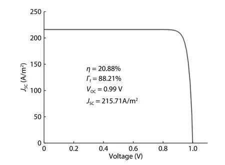
Then, we calculated the influence of nano-sphere refractive index on the conversion efficiency keeping the D and R of 0 and 0.6 μm, respectively, as seen in Fig. 6. The conversion efficiency rapidly increases as the refractive index variation from 1.2 to 1.8, and the higher conversion efficiency can be observed in the refractive index variation range of 1.8-2.2,then the conversion efficiency slowly reduces when the refraction index increases from 2.2 to 3.0. Fig. 7 illustrates the J-V characteristic of optimal GaAs solar cells with distance of adjacent nano-spheres (D), radius (R) and refractive index (n)of 0 μm, 0.6 μm and 2.1, respectively.
Finally, we discuss the tolerance for the three parameters of D, R and n of nano-spheres. It is clearly found from the Fig. 2 that the much poor tolerance is exhibited for the D variation; the conversion efficiency reduces from 20.8% to 18.4%as D increase from optimal value (0 μm) to 1 μm with optimal radius of 0.6 μm, leading to absolute efficiency reduction of 2.4%. However, in the actual fabrication process tightly clustered 2D polymer nano-sphere arrays can be easier to implement using self-assembled manufacture techniques.Fig. 2 also shows that the absolute cell efficiency is varied by less than 1% as the value of R for optimal structure (dark blue line as shown) varies from 0.3 to 1.2 μm, meaning very good manufacturing tolerance. From Fig. 6, it can be found that there is good tolerance for conversion efficiency around the optimal value of refractive index and there is less than 0.2%variation in final cell conversion efficiency for around ±24%variation in the optimal reflective index values of 2.1, which implying that it does not demand high precision processing equipment and the whole nano-sphere array could be fully engineered using self-organized chemical methods.
It should be noted that the highly order two-dimensional nano-sphere array structures could be fabricated on the top surface of GaAs solar cell using monodisperse polystyrene (PS), PS spheres were synthesized with different sizes via emulsion polymerization at different temperature. The refractive index of the PS nano-spheres is around 1.59 at a wavelength of 550 nm, which is suitable for high-throughput and large-area processing by using self-assembled chemical methods[20].

Fig. 5. (Color online) Calculated spectral distribution graph for (a) absorption, (b) reflection and (c) transmission for different R values.

Fig. 6. Illustration of the overall cell efficiency as a function of the refractive index of nano-spheres (n).

Fig. 7. J-V characteristics of the GaAs based solar cells.
4. Conclusion
In this paper, we present our efforts on simulating and analyzing the light trapping in GaAs solar cells using a nanosphere array surface texture due to the simplest and the fastest methods building a two-dimensional photonic crystal structure on the GaAs surface. Based on the scattering and diffraction theory of the photonic crystals, the simulation results show that the distance of adjacent nano-spheres has the great influence on the conversion efficiency and exhibits poor tolerance, the absolutely conversion efficiency is reduced by exceeding of 2% as the D varies from 0 to 1 μm.In addition, the lower conversion efficiency (< 18%) is exhibited and almost remains unaltered when the D is of > 2 μm.The radius (R) of nano-spheres demonstrates much great tolerance. For D = 0, the solar cells exhibit high conversion efficiency (> 20%) and the efficiency is only varied by less than 1% when R is varied in a very wide region of 0.3-1.2 μm.One can also find out that there is good tolerance for efficiency around the optimal value of refractive index (n) and there is only about 0.2% decrease in final cell efficiency for around ±24% variation in the optimal values, which implying that it does not demand high precision processing equipment and the whole nano-sphere array could be fully complemented using self-assembled chemical methods.
Acknowledgements
The authors would like to thank National Nature Science Foundation of China (Grant No. 61871350) and Zhejiang Provincial Department of Education for their financial support of this research (Grant Nos. Y201121882 and Y201225406).
杂志排行
Journal of Semiconductors的其它文章
- Cesium lead inorganic solar cell with efficiency beyond 18% via reduced charge recombination
- Preface to the Special Issue on the Celebration of the 60th Anniversary of Dedicating to Scientific Research of Prof.Zhanguo Wang
- Realization of high-performance tri-layer graphene saturable absorber mirror fabricated via a one-step transfer process
- Quantum cascade superluminescent light emitters with high power and compact structure
- Surface traps-related nonvolatile resistive switching memory effect in a single SnO2:Sm nanowire
- Strain tunable quantum dot based non-classical photon sources
