Charge transfer induced surface enhanced Ramanscattering of single crystal and polycrystal perovskites
2019-10-22YUZhiYUWeiliGUOChunlei
YU Zhi, YU Wei-li*, GUO Chun-lei,2*
(1.The Guo China-US Photonics Laboratory,Changchun Institute of Optics,FineMechanics and Physics,Chinese Academy of Sciences,Changchun 130033,China; 2.The Institute of Optics,University of Rochester,Rochester,NY 14627,USA)
*Corresponding author, E-mail:weili.yu@ciomp.ac.cn, guo@optics.rochester.edu
Abstract: The charge transfer(CT) process plays a key role in the operation of the optoelectronic device system so a better understanding of the interfacial CT property is greatly important. In this paper, Surface Enhanced Raman Scattering(SERS) was utilized to study the interfacial CT property between CuPc and perovskites(single crystal and polycrystalline). The Raman spectra of CuPc adsorbed on the perovskite surface was enhanced. The laser wavelength dependent SERS study indicates that this phenomenon is mainly arising from the CT from the VB band of perovskite to the LUMO band of the CuPc molecules. In comparison, the SERS signal of CuPc molecules adsorbed on a single crystal is much stronger than that on the polycrystalline perovskite. This result indicates that the defect status affects the enhancement ability of the materials. Further study shows that, after the decoration of a thin silver film, the SERS spectra of CuPc on both single crystal and polycrystalline perovskites are further enhanced. The extreme enhancement is not only due to the electromagnetic property of the silver film but also the fact that the SPR of the silver enhances the charge separation of the perovskite, which further promotes the CT process between the substrate and adsorbed molecules. The CT based SERS study shows great potential application value in the field of optoelectronic research.
Key words: SERS;perovskite;charge transfer;CuPc
1 Introduction
Hybrid organic-inorganic perovskite materials have attracted enormous attention for their applications in optoelectronic devices, such as solar cells, photodetectors, light-emitting diodes,etc[1-3]. Their wide applicability is mainly due to their attractive optical and electrical properties including high optical absorption coefficient, high carrier mobility and long carrier diffusion length[4-6]. In optoelectronic devices, perovskite plays the role of absorber or emitter accompanied by the assistance of a hole transport layer(HTL) and electron transport layer(ETL)[7-9]. In solar or photodetector systems, when light is irradiated on the devices, a perovskite layer adsorbs the photons and results in charge separation and free carrier generation. The photon-induced electrons and holes are then transferred into the ETL and HTL separately by the energy gaps of different layers. In order to fabricate high efficiency devices, much effort has been made regarding perovskite film deposition, structure optimization and interface manipulation[10-11]. In addition, several valuable works have also focused on clarifying the charge processes, which is beneficial for understanding the working principles of optoelectronic devices[12-15]. Among all the charge processes, charge transfer at the interface plays a very important role in determining the current-voltage characteristics and the conversion efficiency of the devices[16-17].
Surface Enhanced Raman Scattering(SERS) was first discovered in 1974 by Fleischmann with the observation of extremely enhanced Raman signal of MPY molecules adsorbed on a rough silver electrode[18]. Since then, considerable interest has been given to SERS with different focusses. Such as, mechanism studies, analytical sciences, materials characterization,etc.[19-21]. The most accepted two mechanisms are the electromagnetic mechanism(EM) and the chemical mechanism(CM)[22-23]. The EM mechanism arises from the local surface plasma resonance of the metal surface, while the CM mechanism is caused by the charge transfer(CT) between a substrate and the adsorbed molecules. The CT induced SERS study is mostly carried out on the base of semiconductor materials, such as metallic oxide, 2D materials and quantum dots,etc.[24-27]. As previous work reports, semiconductor based SERS study provides a possibility for analyzing the structure and optoelectronic properties of the semiconductor-molecules interfaces[28-29], such as the size of the semiconductor and excitation laser wavelength dependent CT process on the semiconductors or semiconductor-metal complex SERS active materials[30-31]. Tarakeshwaretal. found that the observed SERS phenomenon on TiO2nanoparticles directly correlates with the electron transit rates across the molecule-TiO2interface[32]. This research is of great importance for better understanding the nature of the CT process in a dye-semiconductor complex and outlinest the role of the SERS vibrational modes in the CT process.In a previous study, we observed the SERS phenomenon on a MAPbCl3single crystal perovskite, which indicates that there is a CT at the perovskite-molecule interface[33]. This study is significant in optoelectronic device studies using the SERS method. However, the adsorbed molecule used in the report is not suitable for fabricating optoelectronic devices.
In this paper, a SERS study was proposed in a dye sensitized perovskite system. A layer of CuPc molecule was deposited on the surface of both single crystal and polycrystalline perovskite. Due to the charge transfer mechanism, the Raman signal of CuPc molecules on the single crystal was noticeably enhanced while the signal of CuPc on the polycrystalline surface can hardly be observed. That is because the crystallinity affects the enhancement ability. Furthermore, a thin layer of Ag was introduced into the dye sensitized perovskite system. The Raman signal of the CuPc on the single crystal perovskite was further enhanced while the polycrystalline system also exhibited obvious enhancement due to both the electromagnetic and charge transfer enhancement mechanism. This study can be used to further study the interface CT process of the dye sensitive perovskite devices.
2 Experiment Section
2.1 Chemical
Lead chloride (PbCl2), Phthalocyanine copper(CuPc), Mercaptopyridine(MPY), dimethyl sulfoxide(DMSO), N,N-Dimethylformamide(DMF), dichloromethane(CH2Cl2) and Ag particles were purchased from Sigma-Aldrich. Chlorine methylamine(MACl) was synthesized as follows[34]:firstly, the mixed solution with 1.2 M methylamine and 1 M hydrochloride acid were stirred for 2 h in an ice bath and then vacuum dried at 50 ℃ for 2 h. After that, the sample was dissolved in ethanol and then filtered using a 0.2 μm PTFE filter. Diethyl ether was then added to the filtered solution to get the MACl powder and then it was vacuum dried at 60 ℃.
2.2 Synthesis of MAPbCl3Perovskite Single Crystal and Polycrystalline Thin Film
Equimolar amounts of MACl and PbCl2was dissolved in the solution of DMSO-DMF(1∶1 by volume) to prepare the MAPbCl3precursor solution with a concentration of 1 M. The solution was then filtered using a 0.2 μm pore size PTFE filter. Then the precursor solution was kept in an oil bath at a temperature of 50 ℃ for 6 h[34].
The perovskite thin films were prepared using a two-step method. The PbCl2(1 M, in N,N-dimetylformamide) solution was spin-coated on cleaned glass slides with a 3 000 r/min for 50 s and then the slides with PbCl2film were heated for 5 min at 60 ℃. Then MACl solution(15 mg/mL, in isoproponal) was dropped onto the PbCl2films after waiting for 30 s and the solution was spin coated to dry.
2.3 Adsorption of SERS Probe Molecules on Perovskite
0.006 g 4-MPY and 0.028 g CuPc was dissolved in 50 mL CH2Cl2separately with a final concentration of 10-3M of each sample. The as-prepared perovskite materials were then immersed into these two solutions for 2 h. After washing and drying, the samples were kept for further measurement.
2.4 Sample Characterization
Raman spectra were collected using a LabRAM HR Evolution Raman spectrometer(HORIBA Jobin Yvon) with excitation laser wavelengths of 473, 532 and 785 nm. The UV-Vis spectral measurements were carried out using a Cary 5000 UV-Vis-NIR spectrometer(Agilent). XRD spectra were collected using BRUKER D8 FOCUS. SEM and EDS analysis were carried out using a scanning electron microscope(Phenom ProX).
3 Result and Discussion
3.1 Characterization of the Perovskite Single Crystal and Polycrystalline Thin Film
Fig.1(color version please see the journal website) shows the surface morphology of the polycrystalline thin film(a) and single crystal perovskite(b). The EDS analysis for the materials takes place inside the red square labeled(color version please see the journal website) in the SEM image and the results show that four elements(C, N, Pb and Cl) are distributed uniformly in both polycrystalline and single crystal MAPbCl3perovskite. Fig.2 shows the XRD spectra of the single crystal perovskite and polycrystalline film, which confirms that both the single crystal and the polycrystalline film possess the single-phase cubic structure with the lattice parametera=5.68 Å[35].

Fig.1 SEM image and EDS analysis of MAPbCl3perovskite polycrystalline thin film(a) and single crystal(b)

Fig.2 XRD spectra of single crystal and polycrystalline perovskite
3.2 UV-Vis Spectra Properties of the Perovskite-MPY System
Fig.3 shows the UV-Vis absorbance spectra of the (a)single crystal and (b)polycrystalline thin film. The MAPbCl3perovskite polycrystalline thin film shows an absorption edge at 407 nm while the single crystal reveals a 428 nm sharp edge, which determines the optical band gap to be 3.05 eV and 2.89 eV separately. However, after the modification of MPY molecules, both of the two perovskite with different crystalline states exhibit a new absorbance band between 450 nm and 500 nm, which shows a new band absorption edge located near 500 nm. As for the MPY molecules themselves, there is hardly any obvious absorption after 425 nm. We can thus conclude that the adsorption of the molecules on the perovskite surface leads to the formation of new band energy at the interface of the perovskite and the MPY molecules.

Fig.3 UV-Vis spectra of single crystal perovskite(a) and polycrystal perovskite(b) before and after modification with MPY molecules compared with the spectra of MPY molecules dissolved in CH2Cl2
3.3 CT Based SERS Study in the Perovskite-MPY System
As in our previous report, the modification of MPY molecules on the single crystal leads to the formation of a new energy level at the interface, which results in a CT between a single crystal and MPY[33]. The interfacial CT process causs the Raman enhancement of MPY molecules under 532 nm laser excitation. However, in the polycrystalline perovskite system, there is nearly no obvious Raman signal achieved. As Fig.4 shows, the Raman spectra of MPY molecules adsorbed on the polycrystalline perovskite only exhibits one weak band located at 1 003 cm-1. This phenomenon can be attributed to that the defect status will affect the SERS results.

Fig.4 Raman spectra of MPY molecules adsorbed on the surface of polycrystalline and single crystal perovskite
However, the lower enhancement property does not mean there is no CT process at the polycrystalline-MPY interface. To further study the CT process of the polycrystalline-MPY system, a thin layer(30 nm) of silver film was added onto the polycrystalline-MPY surface and the Raman spectra of this system were collected. The Raman spectra of MPY molecules in the polycrystalline-MPY-Ag system compared with the Ag film modified with MPY molecules is shown in Fig.5. As the figure shows, the Raman signal of MPY on Ag film was enhanced, which is due to the local surface plasma resonance. In the perovskite-MPY-Ag system, the Raman signal of MPY molecules was further enhanced and the bands at 1 223 cm-1(C-H in-plane wag) and 1 577 cm-1(C-C stretch with deprotonated nitrogen) were selectively enhanced compared to the band at 1 200 cm-1(C-H in-of-plane asym bend) and 1 609 cm-1(C-C stretch with protonated nitrogen). It was reported that, the vibration bands at 1 223 cm-1and 1 577 cm-1can be assigned to the b2mode and the selective enhanced b2mode indicates that a CT process takes place in the system, which is beneficial for Raman enhancement. Thus, we can conclude that the polycrystalline perovskite plays a key role in the Raman enhancement of the MPY molecules.

Fig.5 Raman spectra of MPY powder, MPY on polycrystalline perovskite, MPY on silver film and MPY on the polycrystalline perovskite deposited with a silver film
3.4 SERS Study of the Perovskite-CuPc System
As is well known, the perovskite materials play a key role in optical-electronic response devices. Interfacial CT is also an important part of this process. From the above discussion, we find that SERS can be used to diagnose the interfacial CT process with the modification of proper molecules on the surface of perovskite. However, small molecules(such as MPY) are not suitable enough to promote the interfacial CT due to the large band difference between the LUMO(lowest unoccupied molecule orbital) and HOMO(highest occupied molecule orbital) level of small molecules. Comparatively speaking, some dye molecules(such as CuPc, FePc, N3), which possess a relativly lower band difference, are much more suitable for the fabrication of optical-electronic response devices. In summary, studying the interfacial CT property in perovskite-dye molecule systems is of great importance.
The as-prepared single crystal and polycrystalline perovskite were immersed into a 10-3M CuPc solution. After being washed and dried, the Raman spectra of the sample were collected under a 532 nm excitation laser. As shown in Fig.6, the Raman signal of CuPc on the single crystal surface was noticeably enhanced while a relatively weak signal appeared on the polycrystalline surface.

Fig.6 Raman spectra of CuPc adsorbed on the perovskite single crystal and polycrystalline compared with the Raman signal of CuPc powder
The band assignments of the spectra is listed in Tab.1[36-38]. Compared to the Raman spectra of CuPc powder, the Raman band′s position of the CuPc adsorbed on the perovskite at 594, 678(B1g, in plane full symmetric nonmetal bound N-M stretch and outer ring stretches), 745(B2g, in plane ring symmetric N-M stretch), 828(A1g, in plane full symmetric N-M stretch), 951, 1 037 and 1 140(A1g, in plane symmetric N-M-N bend) remained unchanged while the bands located at 1 339(B1g, in plane full symmetric N-C stretch and ring C-C stretch), 1 449(B2g, in plane ring symmetric outer ring C-C stretch) and 1 525 cm-1(B2g, ring C-C stretch and in plane ring symmetric nonmetal bound N-C stretch) shifted to longer wavelengths. The lower enhancement of the signal on the polycrystalline perovskite can be attributed to stronger defects.
However, it should be mentioned that the Raman signal of CuPc on the polycrystalline surface is weaker than the CuPc powder. It is because of this that only one single layer of CuPc molecules adsorbed on the perovskite surface while far more molecules of CuPc powder were adsorbed at the laser′s focus point for the relative Raman measurement.

Tab.1 Band assignment of the CuPc molecules
3.5 Mechanism of the SERS Enhancement of CuPc adsorbed on Perovskite
As mentioned above, the EM mechanism is mainly due to the laser-induced surface plasmon resonances on the metal cluster surface, which results in a strong local enhancement of the electric field. This can significantly enhance the Raman signal of the molecules adsorbed on or near the metal surface and the enhancement factor is estimated to be as large as 1012-1015.
On the other hand, the CM mechanism is of equal importance in SERS studies[39-40]. For in-stance, the factor contributing to enhancement in metals or semiconductors due to above mechanism is associated with the chemical adsorption of the probe molecule and includes either molecule-metal/semiconductor or metal/semiconductor-molecule CT processes. The application of the Herzberg-Teller theory has been the most comprehensive approach in the study of this effect. The main process could be simply described as the excitation of an electron from a full HOMO to an empty level on the metal/semiconductor band(molecule-metal/semiconductor) or from a full level of the metal/semiconductor to the LUMO. Such conditions are a resonance Raman-like process in which CT between the substrate and the molecule constitutes the intermediate stage.
As mentioned in our previous report[33], the MAPbCl3perovskite do not possess surface plasmons along the excitation region of the laser lines used in these experiments(473 nm, 532 nm and 785 nm) and the mechanism of the SERS phenomenon based on the perovskite materials was attributed to the CT resonance at the interface between perovskite and the adsorbed molecules. To verify this result, the SERS spectra of CuPc on the perovskite were further measured under another two excitation lasers with different wavelengths:473 nm and 785 nm.
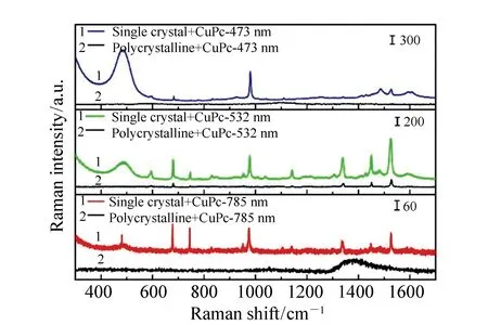
Fig.7 SERS spectra of CuPc adsorbed on single crystal and polycrystalline perovskite under the excitation lasers of 473, 532 and 785 nm
As shown in Fig.7, the SERS spectra of CuPc molecules adsorbed on perovskite exhibit enhancement at different levels. In the single crystal system, the SERS intensity of the CuPc molecules under 532 nm excitation laser undergoes the strongest enhancement compared to the other two excitation laser conditions while in the polycrystalline system, only 532 nm excitation laser can induce SERS enhancement for the CuPc molecules. No SERS signal can be achieved under the other two excitation laser conditions. In addition, it can be found that under the three excitation laser conditions, the single crystal perovskite system shows obvious signs that it is attributed to the vibration of the MAPbCl3, while the polycrystalline hardly results in any observable bands. This further verifies that the less defective the system, the better SERS enhancement. The strongest enhancement occurs under 532 nm excitation and can be attributed to the laser-induced interfacial CT from the VB band of perovskite to the LUMO level of the CuPc molecules.

Fig.8 Laser induced CT processes under the excitation laser of 473, 532 and 785 nm
The CT process is shown in Fig.8. As reported in prior research, the VB and CB bands of MAPbCl3perovskite are located at 5.82 eV and 2.94 eV separately[34]. The LUMO and HOMO level of CuPc is 3.5 eV and 5.2 eV[41]. Under these conditions, the energy difference between the VB band of perovskite and the LUMO level of CuPc is 2.32 eV. This energy difference is well matched with the energy of the 532 nm excitation laser. Thus, the 532 nm excitation laser can induce a charge transfer between the VB band and the LUMO level, which finally results in a SERS enhancement for the CuPc molecules adsorbed on the perovskite. As for the 473 nm excitation laser, the laser energy is 2.62 eV. It is larger than 2.32 eV and cannot match well with energy difference so the 473 nm laser cannot induce CT resonance at the interface.In the case of 785 nm excitation laser, the laser energy is 1.58 eV, which is not enough to excite electron transits from the VB band to the LUMO level. Thus, we can conclude that, the energy of the 532 nm excitation laser matches the energy difference well and it can induce CT at the interface, which results in SERS enhancement for the CuPc molecules adsorbed on the perovskite surface.
3.6 SERS Property of the Perovskite-CuPc-Ag System
It is well known that noble metals are widely used in SERS studies. The surface plasmon resonance(SPR) can produce a strong electromagnetic field on the surface of the materials, which can also be applied elsewhere, such as in photoluminescence[42], biolight emission devices[43]and solar cells[44]. Some recent studies reported that in metal-semiconductor solar cell systems, the SPR-induced dipole acts as an energy level and an enhanced pumping rate for photoelectronic formation and increases the CT efficiency at the interface. Finally, the photoelectric current was increased[45]. We created a thin silver film to study the effect of SPR on the Raman enhancement and interfacial charge transfer property of the CuPc-perovskite system.
Fig.9 shows the SERS spectra of CuPc molecules adsorbed on the perovskite and deposited on 30 nm silver film. After the decoration of silver film, compared to the CuPc-perovskite system, not only were the SERS intensity of CuPc adsorbed on single crystal perovskite significantly enhanced under all the three excitation lasers, but the SERS intensity of CuPc on polycrystalline perovskite films also showed obvious increased. Among all the three excitation laser conditions, the 532 nm laser induced the strongest SERS enhancement. This is because the silver possesses the strongest SPR effect under 532 nm laser excitation. Under 743 nm and 532 nm irradiation conditions, the SERS enhancement mainly arises for two reasons:(1)The SPR induced strong electromagnetism can lead to the enhancement of the signal due to the EM mechanism; (2)The SPR can enhance the charge separation and further increase the charge transfer at the interface. However, under the 785 nm condition, the SERS intensity of CuPc at the single crystal and polycrystalline perovskite are nearly the same. It is because of this that the lower laser energy and weaker SPR effect under 785 nm excitation cannot effectively enhance the interfacial CT. Its SERS enhancement is mainly due to the EM mechanism.
In order to verify the contribution of perovskite to the SERS enhancement, the SERS spectra of CuPc on silver film were further measured. The SERS spectrum of CuPc adsorbed on the silver film was shown in Fig.10. It can be seen from the figure that the SERS signal of CuPc adsorbed on both perovskite and the silver film were enhanced. However, the SERS intensity of CuPc in the perovskite/Ag complex system was further enhanced. Thus, it can be concluded that the SERS phenomenon comes from the double contribution of perovskite and silver film.

Fig.10 SERS spectra of CuPc-perovskite, CuPc-Ag, perovskite-CuPc-Ag and the Raman spectra of CuPc powder
4 Conclusion
In this paper, a SERS study was carried out in perovskite/CuPc and perovskite/CuPc/Ag complex systems. It was found that the spectral intensity of CuPc adsorbed on perovskite can be with CT mechanism. In addition, because of the difference in the level of defects, the single crystal perovskite shows much better enhancement ability than the polycrystalline crystal film. The laser wavelength dependent SERS spectra indicate that the perovskite/CuPc complex system shows the strongest SERS enhancement under 532 nm excitation. This is because the laser energy matches the energy difference of the interface, which induces CT from the VB band of the perovskite to the LUMO level of the molecules. In the perovskite/CuPc/Ag complex system, the laser will induce a surface plasma resonance, which will enhance the charge separation and promote the SERS enhancement. The CT based SERS study of the perovskite/CuPc and perovskite/CuPc/Ag system is helpful for clarifying the interfacial charge transfer process and providing further assistance for the study of optoelectronic response devices.
