TDD-net:a tiny defect detection network for printed circuit boards
2019-09-17RunweiDingLinhuiDaiGuangpengLiHongLiu
Runwei Ding, Linhui Dai , Guangpeng Li, Hong Liu
1Key Laboratory of Machine Perception, Peking University, Shenzhen Graduate School, People’s Republic of China
2Shenzhen Skyworth-RGB Electronic, CO., Ltd., People’s Republic of China
Abstract:Tiny defect detection(TDD)which aims to perform the quality control of printed circuit boards(PCBs)is a basic and essential task in the production of most electronic products.Though significant progress has been made in PCB defect detection, traditional methods are still difficult to cope with the complex and diverse PCBs. To deal with these problems,this article proposes a tiny defect detection network (TDD-Net) to improve performance for PCB defect detection. In this method, the inherent multi-scale and pyramidal hierarchies of deep convolutional networks are exploited to construct feature pyramids. Compared with existing approaches, the TDD-Net has three novel changes. First, reasonable anchors are designed by using k-means clustering. Second, TDD-Net strengthens the relationship of feature maps from different levels and benefits from low-level structural information, which is suitable for tiny defect detection. Finally,considering the small and imbalance dataset, online hard example mining is adopted in the whole training phase in order to improve the quality of region-of-interest (ROI) proposals and make more effective use of data information.Quantitative results on the PCB defect dataset show that the proposed method has better portability and can achieve 98.90% mAP, which outperforms the state-of-arts. The code will be publicly available.
1 Introduction
The printed circuit board (PCB) is essentially a board that mechanically supports and electrically connects electronic components.It is the basic building block of any electronic design and has developed into a very sophisticated component over the years. PCBs are widely used in all but the simplest electronic products. In 2018,the global single-sided PCB market analysis report estimated that the PCB market would reach $79 billion by 2024. Visual defect inspection which ensures PCB product quality is generally the largest cost of PCB manufacturing [1]. In recent years, automatic optical inspection(AOI)system has replaced most of human inspections, which improves the inspection precision and reduces the cost consistency [2]. Although AOI system is more convenient and efficient than human inspection, the false detection rate and the missing detection rate are still too high [3].
Three major challenges exist in PCB defect detection.First,there are a broad range of different PCBs in the real market, different PCBs have different complex wring design rules. As making general algorithms compatible with various PCBs is difficult,instability in the traditional PCB defect detection methods may occur. Second, the categories and characteristics of PCB defects are generally varied. Third, collecting large number of PCB defect samples is extremely difficult in industry, resulting in a data imbalance for some traditional methods.
PCB defects can be divided into two categories:functional defects and cosmetic defects[4].Functional defects can seriously affect the performance of PCB, which may lead to the abnormal usage of PCBs. These defects are the most serious defects. Cosmetic defects mainly affect the appearance of PCB, but also damage its performance in the long run due to abnormal heat dissipation and distribution of current [1]. Among the two categories, there are six kinds of defects which frequently appear in the actual industrial scene. Here, we mainly study these six known and common defects which contain missing hole, mouse bite, open circuit,short, spur, and spurious copper. Some defects examples are shown in Fig. 1. In this figure, defect areas are indicated by thicker and red outlines. Best viewed in colour.
In recent years, various image processing algorithms are widely investigated for PCB defect detection,such as binary morphological image processing [5], similarity measure approach [6], and segmentation-based method [7]. However, these methods require the inspected images to be aligned with the standard sample in defect inspection, suffering from low contrast, uneven brightness or irregular shape. Therefore, it is necessary to build a novel defect detection framework that has strong adaption for diverse defects.
Since 2014, algorithms based on deep-learning have been made significant improvements in object detection, such as faster R-CNN [8], single shot MultiBox detector [9], and You Only Look Once [10]. Deep-learning methods have shown a good performance in automatically extracting features and realising end-to-end control. However, deep-learning algorithms are limited in the field of PCB defect detection due to the local feature property of CNN, while the defect regions usually occupy a tiny portion of a defective PCB image. Therefore, almost no feasible network has been proposed for PCB defect detection until now.Among region-based detectors, Faster R-CNN [8]has shown significant competitiveness in object detection due to its detection accuracy on public benchmarks (COCO [11], PASCAL VOC2007[12]). Faster R-CNN improves the region proposal quality and object detection accuracy by combining the region proposal network with Fast R-CNN [13]. However, for tiny objects, the region-of-interest (ROI) pooling layer which performs on a low-resolution feature map can result in ‘plain’ features while the size of small objects can even be smaller than stride. So it will introduce some challenges while naively employing Faster R-CNN for PCB defect detection. We review the issues why Faster R-CNN is not suitable for small object detection, and redesign the architecture to specifically address them in order to adapt for tiny defect detection. We focus on two challenges:
(i) How to design reasonable anchors?The PCB defect images are different from common images in open-source datasets.The defects only occupy a tiny proportion of a PCB image.However,the general detection methods of R-CNN series often have predefined anchor scales which are suitable for large object detection, such as pedestrian detection and vehicle detection.Thus,a natural challenge is to design reasonable anchors for tiny defects.

Fig. 1 Some defects examples
(ii) How to fuse multi-scale feature maps by redesigning the architecture of Faster R-CNN? Finding a tiny defect is fundamentally challenging because the features of tiny defects will gradually disappear in the feed-forward computation of the backbone ConvNets. Hence, we need to rethink the architecture of Faster R-CNN[8]and Feature Pyramid Network[14]based on the considerations of tiny scale and irregular shape of PCB defects.
Given the aforementioned concerns, we propose a novel tiny defect detection network to tackle the PCB defect detection problem. First, considering the small PCB defect dataset, data augmentation methods are naturally adopted to provide more training data. Adequate training data can effectively avoid overfitting. Second, we propose a novel tiny defect detection network (TDD-Net) which strengthens the relationship of feature maps from different levels and benefits from low-level structural information. Finally, to address the significant actual factory problem, some tricks are explored to enhance the detection performance. More details are presented in Section 4.
Contributions: With aforementioned methods we proposed, the main contributions of this paper can be conducted as:
(i) This paper presents a novel tiny defect detection network(TDD-Net), which can learn better features for tiny defect detection and address some issues of traditional methods. The code will be publicly available.
(ii) This paper first attempts to apply deep-learning algorithms combined with feature pyramid ConvNets to tackle the PCB defect detection problem.
(iii) Extensive experiments are carried out on PCB defect dataset to demonstrate the effectiveness of our proposed network. TDD-Net achieves state-of-the-arts performance on the task of PCB defect detection. Moreover, TDD-Net is easy to be extended to other fields of defect detection, such as fabric defect detection and aluminium defect detection.
2 Related work
In the last decades, different defect detection methods have been proposed in the field of PCB defect detection. Moganti [15]first proposed three categories of PCB inspection algorithms: referential approaches, non-referential approaches, and hybrid approaches.
2.1 Referential methods
The referential methods use a real pixel to pixel(or feature to feature)comparison between a standard PCB image and inspected PCB image. These methods can detect obvious defects like short, open circuit, and missing track.
Image subtraction is the simplest and most direct referential approach by XOR logic operator. The subtraction operation runs fast because it has only two types of pixel values to compare. The advantage of this approach is that it is simple to implement in dedicated hardware and it allows verification of the overall defects in the geometry of PCB [15].
The main difficulty of XOR operation is to determine a precise alignment of the reference image and the inspected image. Consequently, feature matching as an improved classical referential approach has been proposed, feature matching extracts more robust features from whole images and establishes the registration mapping relationship. Generally, the extracted features include points, edges, outlines, and centroid of a particular area, such as HOG,SIFT,and SURF.The SIFT features are robust to scale,rotation, affine, and illumination change. The SIFT feature matching is currently the most effective algorithm in the feature detection and matching algorithms.
Another significant referential method is similarity measure.Gaidhane et al. [6]proposed a symmetric matrix which calculated using the companion matrices of two compared image. The rank of a symmetric matrix is then used as similarity measure metric for defect detection. The numerical value of rank is zero for the defectless and distinctly large for defective images. The advantage of this approach is that the measurement of similarity is taken without computing features such as eigenvalues and eigenvectors.However, it still suffers from environment noise.
In the referential methods, there are several critical practical problems: misalignment, colour variation, reflectivity variation,surrounding variations and fuzzy boundary defect segmentation.Moreover, to obtain such a totally standard PCB image from actual production environment is relatively unrealistic.
2.2 Non-referential methods
Non-referential methods are based on the verification of the general design rules. Nowadays, feature learning by using deep neural networks has been applied to defects recognition and classification. Some superior object detection approaches, such as R-CNN series (R-CNN [16], Fast R-CNN [13], Faster R-CNN[8]), DarkNet [17], SSD [9], and R-FCN [18], show obvious improvements in defect detection.
F. Shahrzad et al. [19]presented a deep-learning approach for automatic detection of rail surface defects. This paper contains three DCNN (for small, medium, and large) structures based on the classical neural network. Soukup. D et al. [20]trained CNNs on a database of photo-metric stereo images of metal surface defects. The classical CNN already distinctly outperforms the model-based approach. However, these traditional CNN methods often use a sliding window to localise the defects, which are difficult to determine the size of window if the input images have different sizes and scales. Y. Cha et al. [21]developed a structural damage detection method based on Faster R-CNN to detect five types of surface damages: concrete cracks, steel corrosion(medium and high levels), bolt corrosion, and steel delamination.Nevertheless, there is almost no defect detection network which has been proposed for PCB defects until now.
2.3 Hybrid methods
The hybrid defect detection techniques combine both referential and non-referential approaches.Z.Qu et al.[22]proposed a new idea to construct a deep convolutional network called PartsNet combing traditional feature processing and deep-learning for automotive engine precision parts defect detection. They also constructed a refining network consisting of several typical traditional methods to improve adaption ability and achieve an end-to-end learning.Thus, PartsNet exploited the strengths of typical feature processing methods such as density slicing, region segmentation, and area filtration to overcome the weakness of deep convolutional networks in detecting small defect regions.
3 Overview of faster R-CNN
In this section, we briefly review the Faster R-CNN detection architecture and naturally redesign some experiment details for PCB defect detection. Faster R-CNN is first proposed to address object detection [8], where given an input image, the network can simultaneously output object bound and class label score at each position. The full pipeline contains two stages: proposal generation and classification. Fig. 2 illustrates the full pipeline.
Generating region proposals is the core task of region proposals,and Faster R-CNN uses k reference boxes (anchors) to k proposals.The anchors have three scales and three aspect ratios, yielding nine anchors at each sliding position.


Fig. 2 Faster R-CNN architecture for object detection
For training RPNs, Fig. 2 shows that RPN is a multi-task that needs to predict object/non-object in proposal and regression bounding boxes. The loss function for an image is defined as [8]:where i is the index of an anchor in a mini-batch and piis the predicted probability of anchor i being an object. The ground-truth labelis 1 if the anchor is positive, andis 0 if the anchor is negative. tiis a vector representing the 4 parameterised coordinates of the predicted bounding box, andis a ground-truth box associated with a positive anchor. For the regression loss, Smooth L1 is used as robust loss function [14]:

For regression, as Faster R-CNN [9], the parameterisations of the 4 coordinates are adopted as following:
where x, y, w, and h denote the two coordinates of the box centre,width, and height, respectively. Variables x, xa, and x∗denote the predicted box, anchor box, and ground-truth, respectively (likewise for y, w, h).
Our goal is to minimise L({pi},{ti}) through back-propagation and stochastic gradient descent (SGD) [23]. For each generated region proposal, features within the region proposal are pooled to a fixed feature map in RoI Pooling layer [13].
Using the pooled feature, a full connected layer then computes object class probability and simultaneously regresses the detection boundaries for each object class.
4 Tiny defect detection network
The proposed TDD-Net follows the Faster R-CNN detection paradigm for PCB defect detection but has three novel changes as shown in Fig. 3. First of all, the CNN model of Faster R-CNN is trained on the PCB defect dataset. During the fine-tuning process,we apply data augmentation techniques and design reasonable anchors. To enhance the detect performance of tiny defects,multi-scale feature fusion strategy is adopted. Online hard example mining is applied in the training phase for improving the quality of RoI proposal. The whole training process follows the end-to-end training paradigm as Faster R-CNN.

Fig.3 Proposed tiny defect detection network architecture which makes use of feature maps on multiple scales.In addition to the bottom-up feature extraction,TDD-Net adds a top-down path which summarises multi-scale feature representations into a single feature map
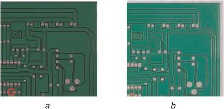
Fig. 4 Defects truncated in the stage of random crop
4.1 Reasonable anchors design and data augmentation
The PCB defect images are different from common images in open-source datasets (COCO [11], PASCAL VOC2007 [12]). The PCB images which collected by industrial camera often have large resolution (e.g. 2,777×2,138), while defects in an image only occupy a tiny proportion of whole image area. At training time,Faster R-CNN uses 3 scales {1282,2562,5122} and 3 aspect ratios {1:1, 2:1, 1:2}, yielding nine anchors at each sliding position, which are not appropriate for detecting tiny defects. With the respect of tiny defects, we must design reasonable anchor.
Inspired by YOLO 9000[24],instead of casually choosing anchor scale, k-means clustering is used on the PCB training set bounding boxes to automatically find reasonable anchor scales. The standard k-means with distance metric is used as follows [24]:

Then the scales with box areas are{152,252,402,602,802}pixels,and four aspect ratios of {2., 3., 4., 5.}. On the other hand, the success of recent deep-learning algorithms greatly relies on large-scale labelled training data. Conversely, without enough training samples, CNNs with numerous parameters have a risk of over-fitting. Large-scale PCB defect dataset is also a limiting requirement due to confidential circuit design and expensive acquisition. Consequently, data augmentation techniques have been proposed to prevent over-fitting while enriching dataset.
In this work, six traditional data augmentation techniques are naturally adopted which including add Gaussian noise, change light, rotate image, flipping, random crop, and shift. The simple operations like adding Gaussian noise or changing light do not required change value of bounding boxes. Nevertheless, while rotating, cropping, and shifting image, the corresponding value of bounding boxes has changed.
The key issues of data augmentation are defects truncated in the stage of random crop (as shown in Fig. 4). Therefore, we need to setup a threshold value and discard these abnormal bounding boxes.
4.2 Multi-scale feature fusion
A deep convolutional network computes a feature hierarchy layer by layer, and through sub-sampling layer, the feature hierarchy has an inherent multi-scale, pyramidal shape. This in-network feature hierarchy produces feature maps of different spatial resolutions, but introduces large semantic gaps caused by different depths. High-resolution feature maps are semantically weak and structurally strong, while low-resolution feature maps are semantically strong. The tiny defect detection can be classified as low-level vision tasks, thus we focus on multi-scale feature fusion.The features of small objects will gradually disappear in the feed-forward computation of the backbone ConvNets, which is quite unfavourable for detecting small objects. Therefore, the high-resolution feature maps of feature hierarchy are important for detecting small objects. TDD-Net adopts feature pyramid architecture [14]which fuses low-resolution features, semantically strong features with high-resolution, structurally strong features via a top-down pathway and lateral connections.
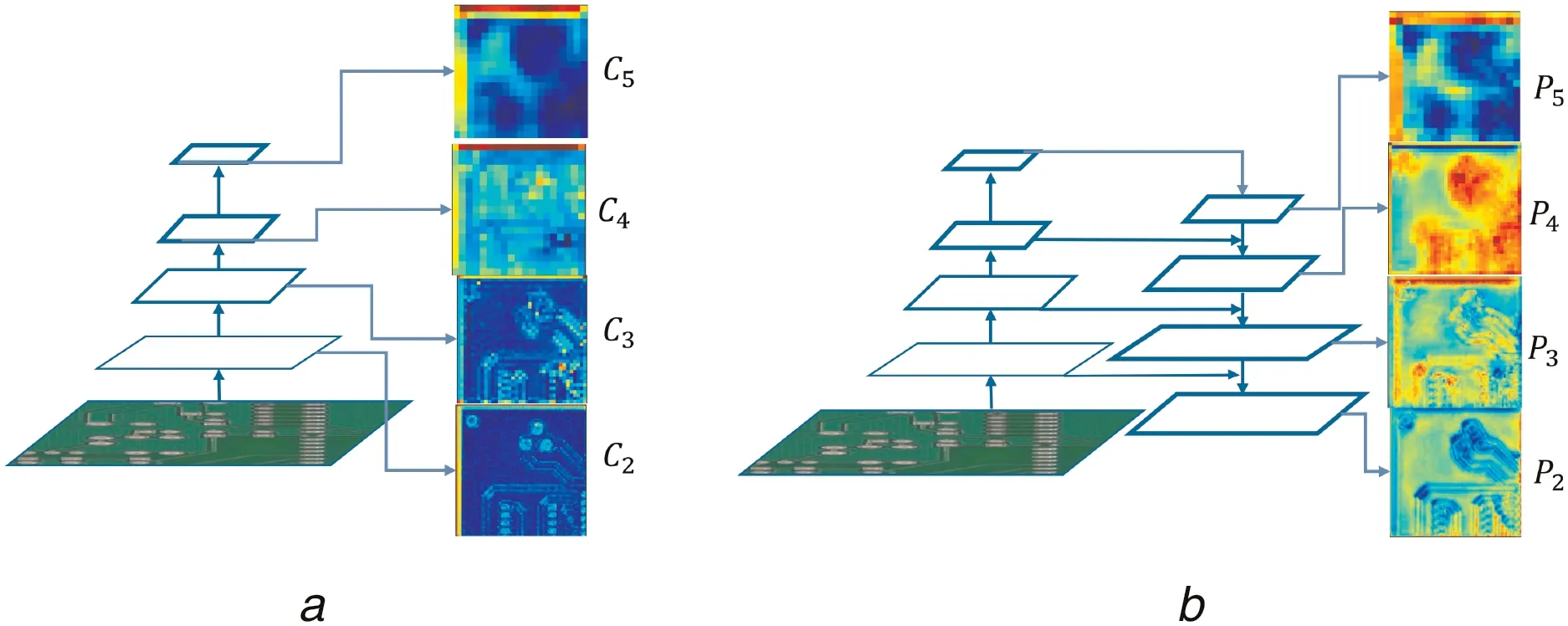
Fig. 5 Feature fusion results on different convolutional layers
First of all, ResNet-101 is used [25]as our backbone ConvNet to extract features. The ResNet-101 models are pre-trained on the ImageNet classification set and fine-tuned on the PCB defect dataset. The ResNets have five residual blocks, and the output of the last residual block is selected as our reference set of feature maps.The outputs of these last residual blocks are denoted as{C2,C3,C4,C5} for conv2, conv3, conv4, conv5 outputs, and note that they have strides of {4, 8, 16, 32} pixels with respect to input image.
Second, the high-resolution feature maps have strong structural information, which helps for detecting small objects. Our top-down feature map is constructed by up-sampling the spatial resolution by a factor of 2, for simplicity, nearest neighbour up-sampling has been selected. Inspired by [14], we propose to concatenate the feature maps both low-level and high-level. Thus,the corresponding bottom-up feature map undergoes a 1×1 convolutional layer in order to reduce channel dimensions. Then,the up-sampled map is concatenated with the corresponding bottom-up map by element-wise addition. For example, the last output feature map {C5} of the last layer undergoes a 1×1 convolutional layer to produce the coarsest resolution map,then the coarsest feature map is up-sampled by a factor of 2, and finally the up-sampled feature map is merged with low-level feature map. Last but not least, a 3×3 convolutional layer is appended on each merged map to generate the final feature map.The final sets of feature map are denoted as {P2,P3,P4,P5},corresponding to {C2,C3,C4,C5}, which are of the same spatial sizes, respectively.
In the stage of assigning RoIs of different scales to the pyramid levels, the level {Pk} of feature pyramid is calculated by [14]:
where 224 is the canonical ImageNet pre-training size,and k0is the target level on which a RoI with w×h=2242.w is the width of RoI and h is the height of RoI.
For a better understanding, feature fusion results on different convolutional layers are visualised in Fig. 5.
4.3 Online hard example mining
We first attempt to apply online hard example mining strategy to the task of PCB defect inspection. Inspired by [26], the readonly RoI network runs a forward pass on the feature map and all RoIs. Then the hard RoI module uses these RoI losses to select examples. Online hard example mining (called OHEM) can be used for training any region-based ConvNets, and it automatically selects hard examples rather than uses several heuristics and hyper-parameters, thus improving detecting efficiency.
4.4 Loss and training
The total loss is a weighted sum of four different losses:rpn_loss_bbox, rpn_loss_cls, fast_rcnn_loss_bbox, and fast_rcnn_loss_cls. A fast R-CNN network has two sibling output layers (cls score and bounding box score). The first outputs a discrete probability distribution (per RoI), p={p0,...,pk}, over k+1 categories. As usual, k is computed by a softmax over the k+1 outputs of a fully connected layer. The second sibling layer outputs bounding-box regression offsets, tk=(tkx,tky,tkw,tkh), for each of the k object classes, indexed by k. The classification loss Lclsis log loss over two classes (object vs. not object), Lclscan be computed by:

where piis the predicted probability of anchor i being an object.p∗i is the ground-truth label.

The regression loss Lregis computed by:

where R represents Smooth L1 function,the definitions of ti,t∗ihave been introduced in Section 3.
5 Experiments and discussions
The experiments are conducted on a computer with 4 NVIDIA GeForce GTX 1080 GPU. The calculation software environment is set with python 2.7.12, CUDA 8.0.44 and cuDNN 5.1.10.
5.1 Dataset
Extensive experiments are carried out on the PCB defect dataset(http://robotics.pkusz.edu.cn/resources/dataset/). The dataset contains 693 PCB defective images and corresponding annotation files. For this dataset, the average pixel size of each image is 2,777×2,138. The PCB defects include 6 classes (missing hole,mouse bite, open circuit, short, spur, and spurious copper). One image contains several defects. The more details of dataset are shown in Table 1.
With the respect of such small dataset, data augmentation techniques are adopted before data training. The images are then cropped into 600×600 sub-images, forming our training set and testing set with 9920 and 2508 images, respectively.The more details of augmented PCB defect dataset are shown in Table 2.
5.2 Evaluation metrics
Two tasks are considered: defects region localisation and defects classification. For defects region localisation, intersection-over-union (IoU) is calculated, and by default an IoU threshold of 0.5 is used for determining true positives on the PCB defect dataset.
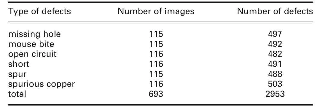
Table 1 Original PCB defect dataset
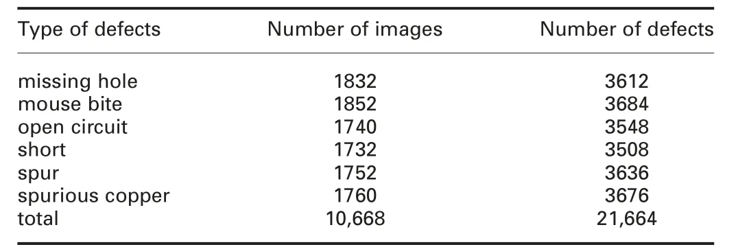
Table 2 Augmented PCB defect dataset
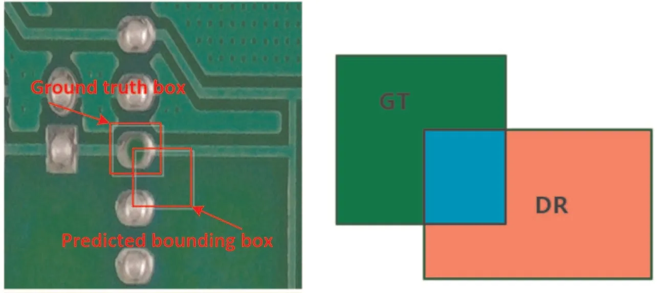
Fig. 6 Three scenarios about the results of ground truth and detection
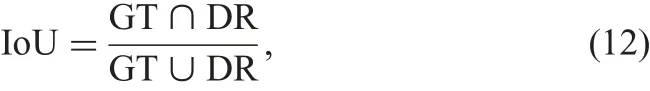
where GT means ground truth, DR means detection results. For better understand, there are three scenarios about the results of ground truth and detection in Fig. 6.
For defects classification, mean Average Precision (mAP) is calculated as evaluation metric. In general, mAP using an IoU threshold of 0.5 is reported as evaluation metric.
5.3 Experimental details and results
Our implementation is based on the TensorFlow Object Detection API. The input image is cropped such that its shorter side has 600 pixels. We perform experiments using a pre-trained ResNet-101 model from [25]. Synchronised SGD is used to train the model on 1 GPU. Each mini-batch involves 2 images per GPU and 512 RoIs per image. A weight decay 0.0001 and a momentum of 0.9 are used. The learning rate is 0.001 for 30k mini-batches. The whole training takes about 7 h on the PCB defect dataset.
Some defects region proposals highly overlap with each other.To reduce redundancy,non-maximum suppression(NMS)is adopted on the proposal regions based on their classification scores. The IoU threshold for NMS is fixed at 0.7, which leaves about 2000 proposal regions per image.
Comparisons with state-of-the-arts: We compare TDD-Net with state-of-the-arts methods on the PCB defect dataset. The results are summarised in Table 3 and Fig. 7, where we compare our method with main stream detection network such as Faster R-CNN with backbone VGG-16 and ResNet-101. TDD-Netachieves the highest mAP when the tIoU threshold is 0.5,demonstrating the effectiveness of TDD-Net and justifying the importance of reasonable anchors design and multi-scale feature fusion. As discussed in Section 4.1 and Section 4.2, the anchor scales of Faster R-CNN are not appropriate for detecting tiny defects. TDD-Net adpots multi-scale feature fusion strategy, it will get structurally strong features which are quite important for detecting tiny defects.

Table 3 Comparison of TDD-Net (proposed) with all recent state-of-the-arts methods on the PCB defect dataset
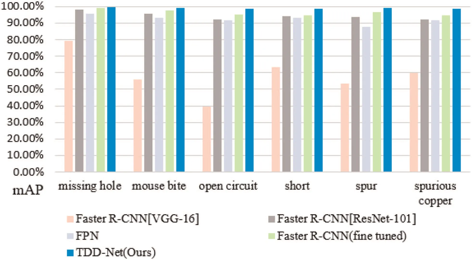
Fig. 7 Comparisons between TDD-Net and state-of-the-arts on the PCB defect dataset
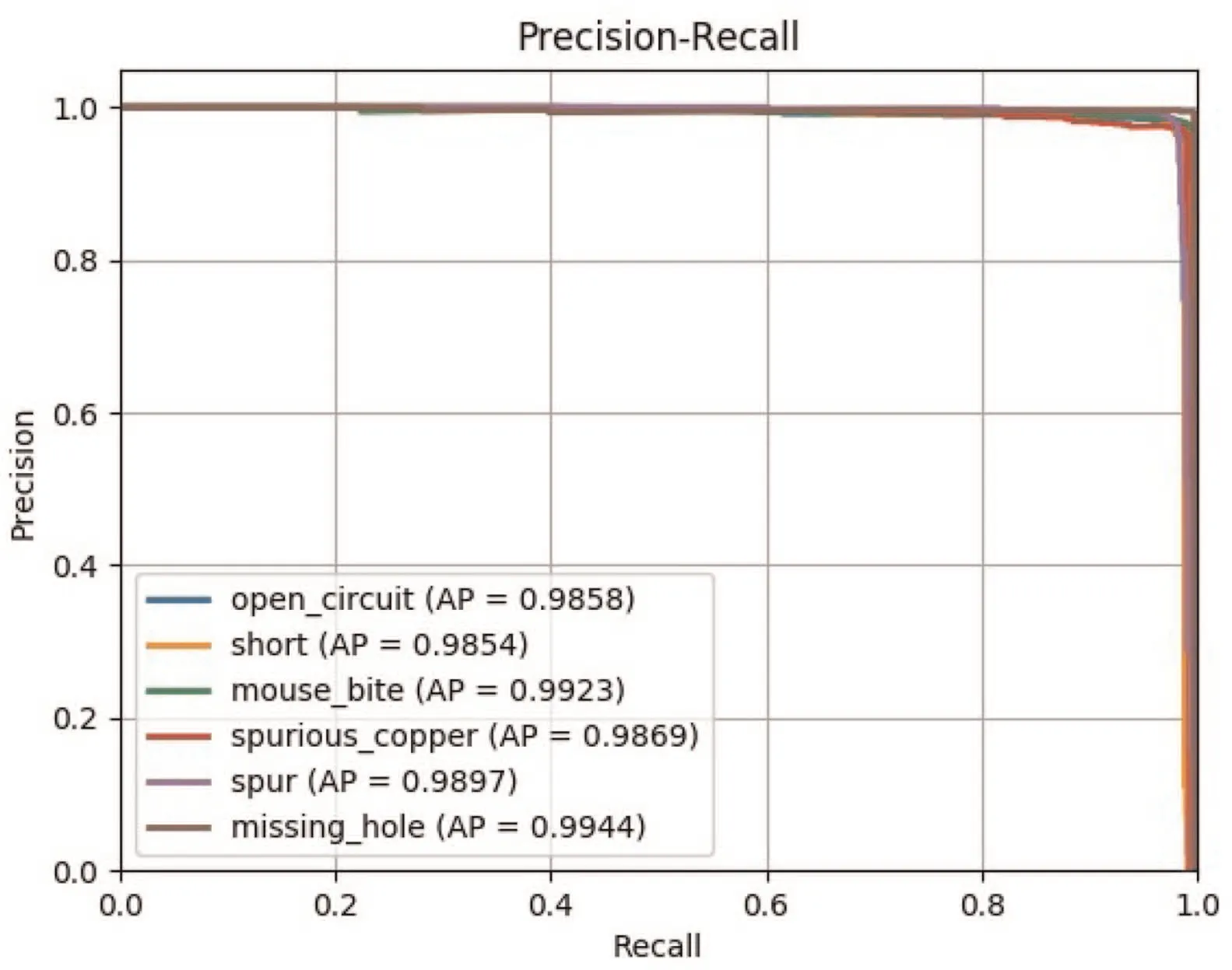
Fig. 8 Precision and recall curve results based on proposed network
Then, we draw Precision–Recall curve to evaluate the performance of defect detection. Fig. 8 compares detection performance among different defect types of PCB on the test set. TDD-Net achieves the superior performance compared with other state-of-the-arts. The mean average and precision is 98.90%. Examples of defect inspection results are presented in Fig. 9.
Ablation experiments: To investigate the behaviour of reasonable anchors design, multi-scale feature fusion and OHEM, we validate the design by comparing four ablation experiments: (i) a naïve Faster R-CNN using ResNet-101; (ii) faster R-CNN using ResNet-101 with anchor fine-tuned; (iii) the addition of multi-scale feature fusion based on former design; and (iv) the addition of online hard example mining.
The ablation experiments results are reported in Table 4.From the table, we can see that the original algorithm (Faster R-CNN with ResNet-101) performs worst, since it relies on the last level feature map which has wilder receptive field and is not suitable for detecting small defects. The algorithm (Original+Reasonable anchors) performs better than original algorithm, but still suffers from misaligned receptive fields; TDD-Net (Original+Reasonable anchors+Multi-scale feature fusion+online hard example mining)outperforms the others, as it combines structurally strong features with semantically strong features, which is help for detecting tiny defects.

Table 4 Ablation study on TDD-Net (ours)
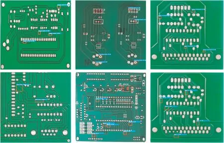
Fig. 9 Defect detection results using the proposed TDD-Net (best viewed in color)
6 Conclusion
This paper presents a TDD-Net, a clean and simple network that aims to perform the quality control of PCBs. To tackle with the problems of low efficiency, high false detection rate,and high missing detection rate, this paper first attempts to apply deep-learning algorithms combined with feature pyramid ConvNets to PCB defect detection problem. TDD-Net has three novel changes to adapt to tiny defect detection. First, experiments demonstrate that reasonable anchors design can obtain more precision IoU scores to accurately locate defects. Second, it can extract better features of tiny defects through feature pyramids.Finally, TDD-Net adopts online hard example mining in the whole training stage to improve the quality of RoI proposals. In these ways, extensive experimental results on the PCB defect dataset demonstrate that TDD-Net achieves better mAP of 98.90% than state-of-the-arts. Ablation studies verify the robustness of TDD-Net. Moreover, TDD-Net has strong expansibility and can be easily extended to other fields, such as fabric defect detection and aluminium defect detection.
Future works will include: (i) exploring zero-shot learning methods due to small training dataset; (ii) optimising of networks and post-process methods; and (iii) extending TDD-Net to more types of PCB defects.
7 Acknowledgments
This work is supported by Specialised Research Fund for Strategic and Prospective Industrial Development of Shenzhen City (No.ZLZBCXLJZI20160729020003).
8 References
[1]Putera,S.,Ibrahim,Z.:‘Printed circuit board defect detection using mathematical morphology and matlab image processing tools’. Int. Conf. on Education Technology and Computer (ICETC), Shanghai, China, June 2010, pp. 359–363
[2]Chin,R.T.,Harlow,C.A.:‘Automated visual inspection:A survey’,IEEE Trans.Pattern Anal. Mach. Intell., 1982, PAMI-4, pp. 557–573
[3]Deng, Y.S., Luo, A.C., Dai, M.J.: ‘Building an automatic defect verification system using deep neural network for pcb defect classification’. Int. Conf. on Frontiers of Signal Processing (ICFSP), Poitiers, France, September 2018,pp. 145–149
[4]Wu, W.Y., Wang, M.J., Liu, C.M.: ‘Automated inspection of printed circuit boards through machine vision’, Comput. Ind., 1996, 28, (2), pp. 103–111
[5]Malge, P.S., Nadaf, R.S.: ‘PCB defect detection, classification and localization using mathematical morphology and image processing tools’, Int. J. Comput.Appl., 2014, 87, (9), pp. 40–45
[6]Gaidhane,V.,Hote,Y.,Singh,V.:‘An efficient similarity measure approach for pcb surface defect detection’, Pattern Anal. Appl., 2018, 21, (1), pp. 277–289
[7]Kaur,B.,Kaur,G.,Kaur,A.:‘Detection and classification of printed circuit board defects using image subtraction method’. Recent Advances in Engineering and Computational Sciences (RAECS), Chandigarh, India, 2014, pp. 1–5
[8]Ren, S., He, K., Girshick, R., et al.: ‘Faster r-cnn: towards real-time object detection with region proposal networks’, Pattern Analysis Mach. Intell., 2017,39, (6), pp. 1137–1149
[9]Liu, W., Anguelov, D., Erhan, D., et al.: ‘Ssd: single shot multibox detector’.Computer Vision – ECCV 2016, Amsterdam, Netherlands, 2016, pp. 21–37
[10]Redmon, J., Divvala, S., Girshick, R., et al.: ‘You only look once: unified,real-time object detection’. IEEE Conf. on Computer Vision and Pattern Recognition (CVPR), Las Vegas, November 2016, pp. 779–788
[11]Lin, T.-Y., Maire, M., Belongie, S., et al.: ‘Microsoft coco: common objects in context’, ArXiv.org (2015): ArXiv.org, 21 February 2015
[12]Everingham, M., Eslami, S., Gool, L., et al.: ‘The pascal visual object classes challenge: A retrospective’, Int. J. Comput. Vis., 2015, 111, (1),pp. 98–136
[13]Girshick, R.: ‘Fast R-CNN’. IEEE Int. Conf. on Computer Vision (ICCV),Santiago, America, December 2015, pp. 1440–1448
[14]Lin, T.Y., Dollar, P., Girshick, R., et al.: ‘Feature pyramid networks for object detection’. Computer Vision and Pattern Recognition (CVPR), Hawaii,America, July 2017, pp. 936–944
[15]Moganti,M.,Ercal,F.:‘Automatic pcb inspection systems’,Potentials,1995,14,(3), pp. 6–10
[16]Girshick,R.,Donahue,J.,Darrell,T.,et al.:‘Rich feature hierarchies for accurate object detection and semantic segmentation’. Computer Vision and Pattern Recognition (CVPR), Columbus, America, June 2014, pp. 580–587
[17]‘Darknet: Open source neural networks in c’. Available at http://pjreddie.com/darknet/, accessed 15 December 2018
[18]Dai, J., Li, Y., He, K., et al.: ‘R-fcn: object detection via region-based fully convolutional networks’. ArXiv.org (2016): ArXiv.org, 21 June 2016
[19]Faghih-Roohi, S., Hajizadeh, S., Nunez, A., et al.: ‘Deep convolutional neural networks for detection of rail surface defects’. Int. Joint Conf. on Neural Networks (IJCNN), Vancouver,Canada, July 2016, pp. 2584–2589
[20]Soukup, D., Huber-Mork, R.: ‘Convolutional neural networks for steel surface defect detection from photometric stereo images’. Int. Symp. on Visual Computing, 2014, vol. 8887, pp. 668–677
[21]Cha,Y.,Choi,W.,Suh,G.,et al.:‘Autonomous structural visual inspection using region-based deep learning for detecting multiple damage types’,Comput.-Aided Civ. Infrastruct. Eng., 2018, 33, (9), pp. 731–747
[22]Qu,Z.,Shen,J., Li, R.,et al.: ‘Partsnet:A unified deep network for automotive engine precision parts defect detection’. ArXiv.org (2018): ArXiv.org, 29 October 2018
[23]Lecun, Y., Boser, B., Denker, J.S., et al.: ‘Backpropagation applied to handwritten zip code recognition’, Neural Comput., 1989, 1, (4), pp. 541–551
[24]Redmon, J., Farhadi, A.: ‘Yolo9000: better, faster, stronger’. IEEE Conf. on Computer Vision and Pattern Recognition (CVPR), Hawaii, America, July 2017, pp. 6517–6525
[25]He,K.,Zhang,X.,Ren,S.,et al.:‘Deep residual learning for image recognition’.IEEE Conf. on Computer Vision and Pattern Recognition (CVPR), Las Vegas,America, June 2016, pp. 770–778
[26]Hrivastava, A., Gupta, A., Girshick, R.: ‘Training region-based object detectors with online hard example mining’. IEEE Conf. on Computer Vision and Pattern Recognition (CVPR), Las Vegas, America, June 2016,pp. 761–769
杂志排行

CAAI Transactions on Intelligence Technology的其它文章
- Three-stage network for age estimation
- Channel-wise attention model-based fire and rating level detection in video
- New shape descriptor in the context of edge continuity
- Efficient discrete firefly algorithm for Ctrie based caching of multiple sequence alignment on optimally scheduled parallel machines
- Convolutional neural network based detection and judgement of environmental obstacle in vehicle operation
- Visibility improvement and mass segmentation of mammogram images using quantile separated histogram equalisation with local contrast enhancement