Recent advances in Ga-based solar-blind photodetectors∗
2019-02-25MingshengXu徐明升LeiGe葛磊MingmingHan韩明明JingHuang黄静HuayongXu徐化勇andZaixingYang杨再兴
Ming-sheng Xu(徐明升),Lei Ge(葛磊),Ming-ming Han(韩明明),3,Jing Huang(黄静),Hua-yong Xu(徐化勇),and Zai-xing Yang(杨再兴),3,‡
1 School of Microelectronics,Shandong University,Jinan 250100,China
2 School of Mechatronics Engineering,Guizhou Minzu University,Guiyang 550025,China
3 Shenzhen Research Institute of Shandong University,Shenzhen 518057,China
Keywords:solar-blind photodetector,AlGaN,Ga2O3
1.Introduction
In the past decades,Ga-based III-V semiconductors have attracted much attention in the fields of next-generation electronics and optoelectronics.[1-14]In the field of optoelectronics,Ga-based ultraviolet(UV)photodetectors have attracted much attention for their applications in industry and our daily life.UV light from the sun at wavelengths between 240 nm to 280 nm is almost totally absorbed by the atmospheric ozone layer and is called solar-blind radiation because of the absence of light at the surface of the earth.The solar-blind photodetectors attract much attention from scientists for its applications in flame detection,ozone monitoring,environmental analysis,and missile tracking.[15-19]Si material has some limitations in UV detections because of its low bandgap energy.Zn x Mg1-x O[20-22]and Zn x Ga1-x O[23,24]semiconductor materials are explored for solar-blind photodetectors(PDs).AlxGa1-xN material is expected to be a promising alternative for solar-blind light detection.[25-29]The band gap of ternary AlxGa1-xN alloy can be adjusted from 3.4 eV to 6.2 eV by changing the Al composition.When the Al content x is larger than 0.4,the cut-off wavelength is smaller than 280 nm and an AlGaN-based solar-blind UV PD is obtained. Although the growth process of III-nitride materials are studied in detail,the crystalline quality of high-Al content AlGaN layer is still an important issue,which severely restricts the performance of AlGaN-based solar-blind UV PD.[30]A metal-semiconductor-metal(MSM)structure is the most common AlGaN-based photodetector.[31,32]It has many advantages,such as a simple fabrication process and easy monolithic integration.AlGaN avalanche photodiodes(APDs)have perfect UV photodetection performance because of their weak light signal detection ability.[33-35]Ga2O3is another Ga-based semiconductor material and can be used for solar-blind photo-detection because of its wide energy band gap(∼4.9 eV).[36-38]The Ga2O3film can be grown by many methods,such as metal-organic chemical vapor deposition(MOCVD),[39,40]molecular beam epitaxy(MBE),[41,42]chemical vapor deposition(CVD),[43]and sputtering.[44]In fact,mechanical exfoliation from a single crystal substrate is a novel method to obtain high quality Ga2O3film.[45]Recently,Ga2O3and otheroxide-based nanowiresand nano flowerswere reported to detect the solar-blind light.[46,47]
AlGaN and Ga2O3are the two most used materials for solar-blind photo detections.In this paper,we review stateof-the-art research work on the Ga-based solar-blind UV PDs.The crystal quality improvement and device structure design of AlGaN and Ga2O3-based photodetectors are discussed in detail.First,we present some typical research work about AlGaN-based solar-blind UV PDs,including nucleation layer optimization,MSM structure technology improvement,and APDs performance enhancement.Then we discuss the recent progress of Ga2O3-based UV PDs.The PDs based on Ga2O3film, flakes,and nanostructures are surveyed in detail.
2.AlGaN-based solar blind photodetectors
The peak photo response wavelength of AlGaN material is determined by the aluminum(Al)composition,which is about 40%in order to obtain solar-blind photodetectors.The crystalline quality of high Al-content AlGaN determines the performance of AlGaN-based solar-blind PDs.Aluminum nitride(AlN)single crystal is an ideal substrate for AlGaN-based PDs because of its wide band gap energy and good lattice matching with gallium nitride.[48]However,the AlN bulk substrate has a small size and high price,which limits its wide application in AlGaN-based devices at present.Due to the lack of homogeneous substrate,the heteroepitaxial growth of AlN on a sapphire substrate(so-called AlN template)was used for AlGaN material growth.[49-52]The growth temperature plays an important role in AlN layer growth.Chen et al.grew AlN template by high-temperature metal-organic chemical vapor deposition and studied the effects of the nucleation layer growth temperature.[51]Three samples were designed,denoted as samples A,B,and C,with nucleation temperatures of 880°C,950°C,and 1020°C.The in situ monitoring curves versus time of the three samples are shown in Fig.1(a).The crystalline qualities of the three samples were evaluated by high-resolution x-ray diffraction(HR-XRD)rocking curves.The full width at half maximum(FWHM)values of(002)and(102)planes are calculated from rocking curves and are shown in Fig.1(b).The results reveal that sample B with 950°C nucleation layer performed at the highest quality.
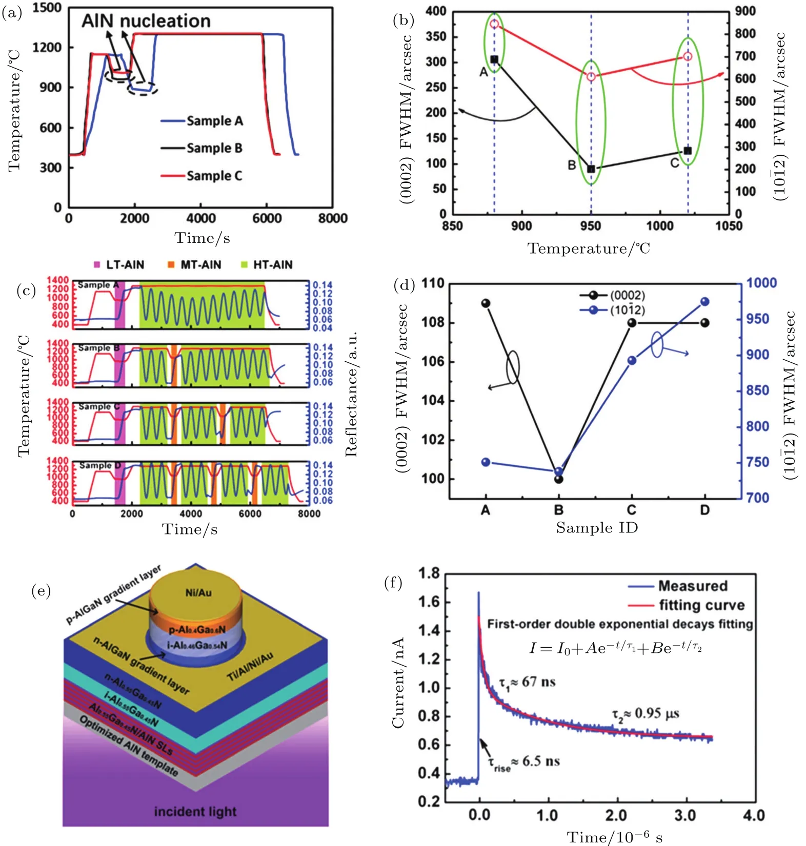
Fig.1.(a)In situ monitoring temperature curves versus time and(b)FWHM values of the samples with different nucleation temperature;[51](c)in situ monitoring temperature and reflection curves versus time and(d)FWHM values of the samples with different MT-AlN interlayers;(e)schematic diagram and(f)decay edge of the transient spectral response of AlGaN-based PD with one MT-AlN interlayer.[49]
A mesothermal AlN(MT-AlN)interlayer was approved to improve the crystalline quality of AlN template in Ref.[49].The authors grew four AlN template samples.Sample A was grown by a conventional two-step method,with 35-nmthick low-temperature(LT)AlN nucleation layer and a 1-µmthick high-temperature(HT)AlN layer.The samples B,C,and D used one,two,and three middle temperature(MT)AlN interlayers among the HT-AlN layers,respectively.Figure 1(c)shows the in situ monitoring temperature and reflectance curves versus time for the AlN template samples.The FWHM values of(002)and(102)planes are calculated from rocking curves and are shown in Fig.1(d).It is obvious that sample B has the lowest FWHM values and best crystalline qualities according to Fig.1(b).The results demonstrate that a single MT-AlN interlayer is the best way to improve the AlN template crystalline quality.In order of confirm the optical-electrical properties of AlGaN material on AlN template,an AlGaN-based ultra-violet photo-detector(UVPD)device on AlN template was fabricated,as shown in Fig.1(e).The optimized AlN template with one MT-AlN interlayer was used in this device.Figure 1(f)shows the current decay curve under zero-bias.The results show that the UVPD device exhibits low dark current and good response speed.
Actually,the device structures also play an important role in the performance of the UVPDs.AlGaN MSM photodiode is an attractive candidate for UV light detection because of its simple fabrication process and suitability for the monolithic integration of an optical receiver.[53]Gökkavas et al.designed MSM photodetectors with beeline interdigitated figures(sample 1a)and circular interdigitated figures(sample 1b),as shown in Fig.2(a).[56]Figure 2(b)shows the corresponding spectral dependence of the photo-response for the two devices.The two devices exhibited sharp cut-off responsivity at about 365 nm.The peak responsivity reached 101.8 A/W for sample 1a and 88.6 A/Wforsample 1b atbias voltage of50 V.The significant high responsivity values reveal that the samples have a gain of about 700 that can be attributed to the photoconductive gain mechanism in MSM PDs.Chen et al.proposed a novel PD structure with low-temperature(LT)AlN layer and inductively coupled plasma(ICP)recessed electrodes.[57]The new structure could improve the photocurrent and decrease the dark current.Figure 2(c)shows the schematic structure of the designed sample.The dark I-V curves and photocurrent of the conventional MSM,MSM with LT-AlN cap layer,and MSM with LT-AlN and recessed electrodes are shown in Figs.2(d)and 2(e).The dark current of the conventional AlGaN MSM photodetector was 8.3×10⁻⁹A at bias voltage of 5 V.The LTAlNcap layerhelped to reduce the dark currentofthe photodetector to 1.1×10⁻¹²A.The almost four orders of magnitude smaller dark current was attributed to the thicker and higher potential barrier of LT-AlN cap layer.Walde et al.studied the in fluence of open-core threading dislocations on the performance of AlGaN photodetectors.[54]The two-dimensional electron gas layer was beneficial to increase the photosensitivity of AlGaN MSM photodetector.[55]
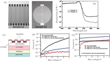
Fig.2.(a)Microphotographs and(b)spectral responsivity curves of MSM photodetectors for samples 1a and 1b at 50 V;[56](c)schematic structure,(d)dark I-V characteristics,and(e)photocurrent of AlGaN MSM photodetectors.[57]
AlGaN-based avalanche photodiode is another important solar-blind UVPD,which can detectvery weak UVsignalsand has high gain and low noise.[58]The p-i-n solar-blind APD contains sapphire substrate,AlN buffer layer,n-AlGaN layer,i-AlGaN layer,and p-AlGaN layer.[59,60]The unintentionally doped i-AlGaN layer was used as the absorption and multi-plication layer.Huang et al.proposed a composition graded p-type AlGaN layer and a p-type GaN layer to reduce the contact resistance of AlGaN-based APD with separate absorption and multiplication(SAM)structure.[61]Figure 3(a)shows the schematic diagram of the designed APD sample.The I-V curves of the APD in dark and UV illumination conditions are shown in Fig.3(c).The dark current of the device is as low as about 0.3 pA at-20 V and exponentially increases with the reverse bias and reaches 50 nA at-75 V.Figure 3(c)also plots the gain values dependent on the reverse bias voltage.The maximum value of the multiplication reaches about 3000.Shao et al.used high/low-Al-content AlGaN layer instead of the conventional high-Al-content AlGaN homogeneous layer to improve the gain of AlGaN APD with SAM structures.Figure 3(c)shows the reverse I-V curves of the APD device under dark and tungsten light illumination conditions.[62]The dark current and light current slowly improve as the reverse voltage increases,and sharply rise when the applied voltage reaches 101 V.The gain curve reveals thatthe maximum multiplication gain reaches up to 5.5×10⁴,which is higherthan thatof a conventional APD.The external quantum efficiency(EQE)was measured under back illumination,as shown in Fig.3(d).The maximum EQE of the device increases from 6.9%to 95.8%with the increase of the reverse voltage.The wavelength corresponding to the peak EQE value is about 275 nm,which is the solar blind region.
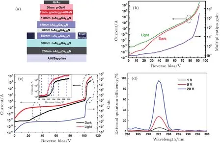
Fig.3.(a)Schematic structure and(b)reverse I-V curves of AlGaN-based avalanche photodetector with grading p-AlGaN;[61](c)I-V curves and(d)quantum efficiency of AlGaN APD with high/low-Al-content AlGaN layer.[62]
3.Ga 222O 333-based solar blind photodetectors
Although the bandgaps of all five crystal phases of Ga2O3lie in the solar-blind ultraviolet waveband,that is,5.2 eV for α-Ga2O3,[63]4.9 eV for β -Ga2O3,[64]4.54 eV for γ-Ga2O3,[65]4.62 eV for κ-Ga2O3,[66]and 4.27 eV for ε-Ga2O3,[66]the most stable phase of β-Ga2O3[67,68]is considered to be the optimal channel materials for solar-blind UV photodetection.Ga2O3PDs have low theory dark current[69,70]compared with other multi-element alloy materials.[71,72]There are several methods to grow Ga2O3active layers,such as metal-organic chemical vapor deposition,[73]molecular beam epitaxy,[74]magnetron sputtering,[75]and mechanical exfoliation from bulk single crystals.[76]Guo et al.grew Ga2O3film with a thickness of 250 nm on(100)p-type silicon substrate by pulse laser deposition(PLD)technology.[77]Ti/Au and Au electrodes were deposited on the Ga2O3film and the Si substrate.The schematic diagram of the Ga2O3/Si heterojunction structure is shown in Fig.4(a).The log-scale currentvoltage(I-V)curves of the device in dark,365-nm UV light,and 254-nm UV light are measured by Keithely 2450,as plotted in Fig.4(b).The I-V curves of Ga2O3/Si heterojunction reveal a typical rectifying characteristic.The light current of the device increased from 8.5×10⁻⁷A to 8.0×10⁻⁴A when the voltage changed from-3.0 V to 3.0 V,corresponding to the I254/Idarkratio of 940.However,the light current is about 5.3×10⁻⁶A under 365-nm UV light,and the I365/Idarkratio is 6.2.The results demonstrate that the Ga2O3/Si photodetector is more sensitive for 254 nm than for 365 nm.Guo et al.grew Ga2O3epitaxial thin film on sapphire substrates by laser MBE method under various temperatures and oxygen pressures.[74]Ti/Au interdigital electrodes were deposited on Ga2O3film and annealed at 300°C for 10 min.Figure 4(c)shows the schematic diagram of the device with MSM structure.The electrodefingers were 200-µm wide,2800-µm long,and with a 200-µm spacing gap.The time-dependent photo response of the Ga2O3detector to 365-nm and 254-nm illumination by on/off switching under 10 V is shown in Fig.4(d).The current increases by more than one order of magnitude,from 128 nA of dark conditions to 1460 nA when the 254-nm UVlightisturned on.In contrast,the currentslightly increases to approximately 300 nA under 365-nm UV illumination.The data demonstrate that the MBE-grown Ga2O3film shows good responsivity to the 254-nm UV light and potential application in solar-blind sensitivity.Oh et al.fabricated Ga2O3-based solar-blind photodetector with a planar structure by MOCVD technology.[73]The fabrication process of the photodetector with circle MSMstructure includes Ga2O3film growth,Si-ion implantation,activation annealing,and electrode deposition.Figure 4(e)shows the optical microscope image of the fabricated device with circle MSM structure.The time-dependent photo response curves of the device were measured by an Agilent 4155 C semiconductor parameter analyzer and are shown in Fig.4(f).The ratio of the photocurrent under 254-nm and 365-nm illumination is9.4.The resultsshow thatSi-implanted Ga2O3thin- film photodetector grown by MOCVD have good photo response properties.
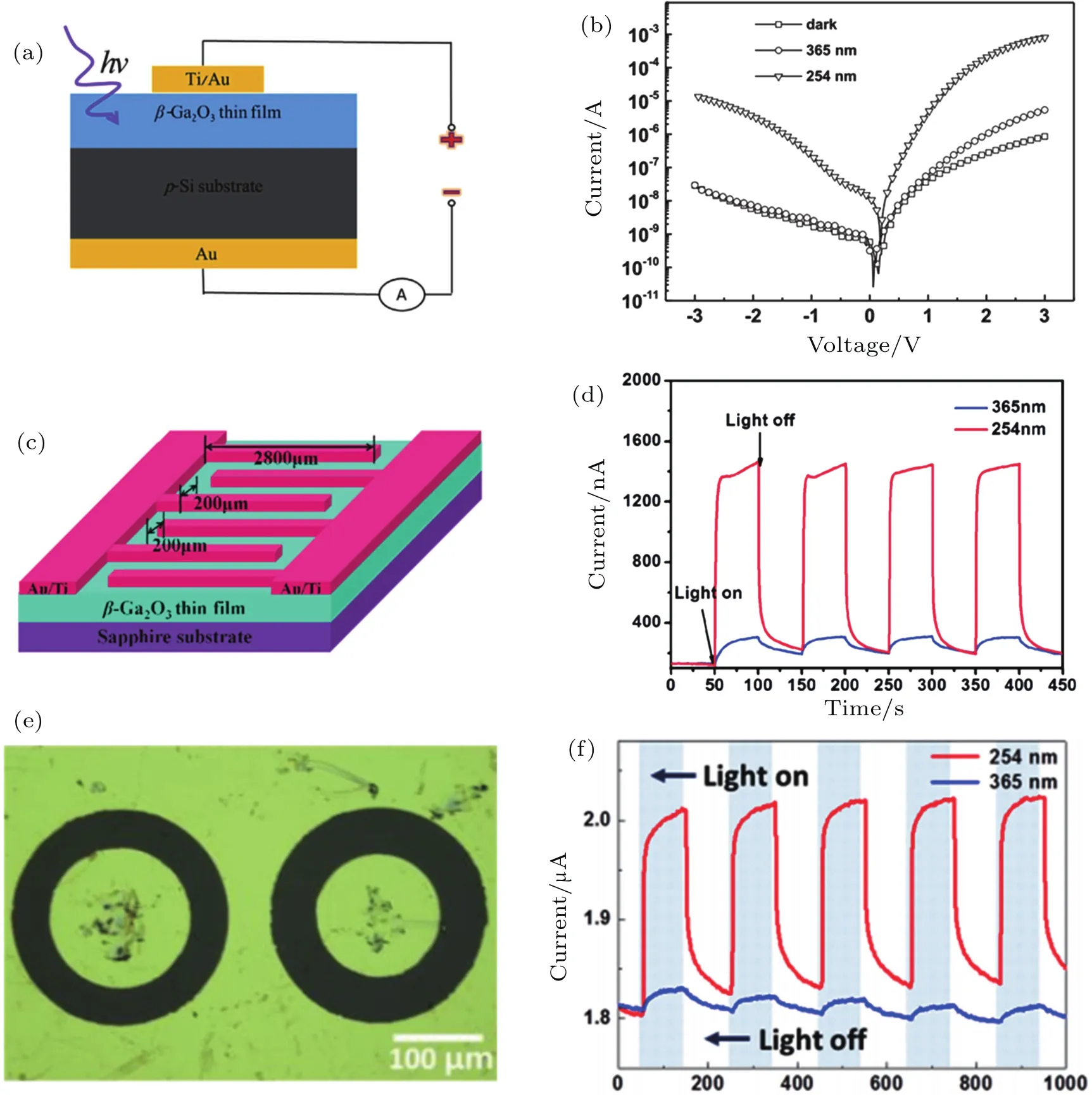
Fig.4.(a)Schematic diagram and(b)current-voltage curves of Ga2O3 photodetector grown by PLD;[77](c)Schematic diagram and(d)currenttime curves of Ga2O3 photodetector grown by LMBE;[74](e)optical microscope image and(f)time-dependent current curves of Ga2O3 detector grown by MOCVD.[73]
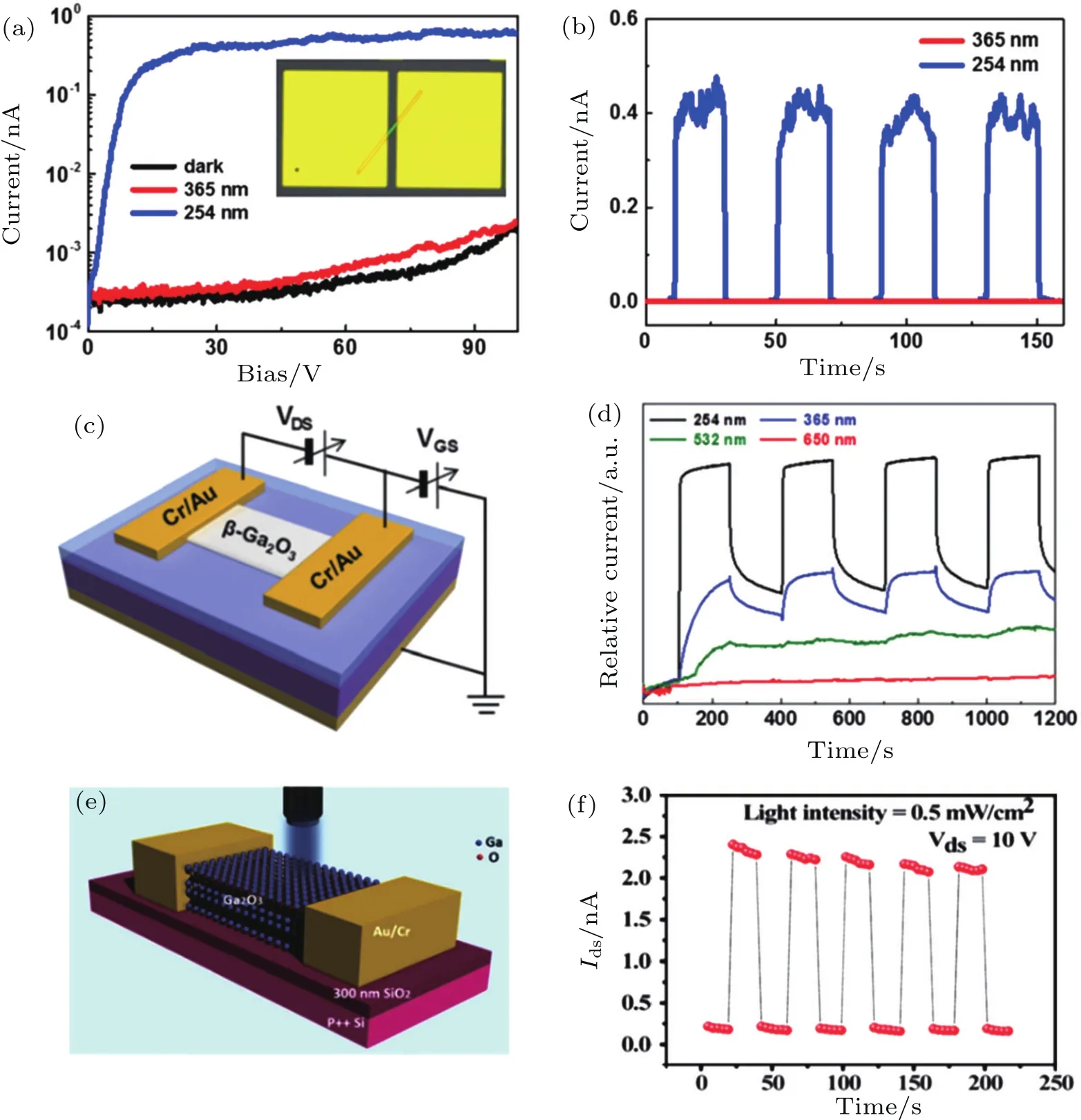
Fig.5.(a)Current-voltage curves and(b)current-time curves of Ga2 O3 flakes MSM PDs;[80](c)schematic diagram and(d)time-dependent photo response properties of the device;[64](e)schematic and(f)stability of photo switching of back gate 2D Ga2O3 solar blind PDs.[83]
Although Ga2O3can be grown by various growth methods,it is still difficult to obtain high quality epitaxial Ga2O3films.Quasi-two-dimensional Ga2O3flakes mechanically exfoliated from a single crystalline substrate[64,78,79]have excellent crystalline quality and could enhance the performance of solar-blind PDs.Oh et al.exfoliated highly crystalline Ga2O3micro- flakes and fabricated MSM solar-blind PDs.[80]The optical microscope image of the device is shown in the inset of Fig.4(a).The current-voltage characteristics under dark,254-nm,and 365-nm UV illuminations are plotted in Fig.4(a).The dark current was approximately 10-14A,which is attributed to the formation of a Schottky barrier between the metal contacts and Ga2O3film.The photo current increased to 0.38 nA when exposed to 254 nm,and revealed no response under 365-nm UV illumination.Figure 4(b)plots the time-resolved current of the Ga2O3PDs,measured by periodically turning on and off the UV light.There was no response when the device was exposed to the wavelength of 365 nm.In contrast,the current rapidly increased and saturated under 254-nm illumination,after which it sharply returned to the initial value as the UV light was turned off.The quasi-two-dimensional(2D)Ga2O3-based back-gate field-effect transistor(FET)was also used as solar-blind photodetector.[64,81,82]The 2D Ga2O3flake using mechanical exfoliation was transferred to SiO2/Si substrate and deposited Cr/Au as source and drain pads.The p-type Si substrate was used as back gate.Figure 5(c)shows the schematic of the device.The space between the two Cr/Au pads was 9µm.The time-dependentphoto response properties were measured by a semiconductor parameter analyzer under various illumination conditions,as shown in Fig.5(d).The results reveal that the Ga2O3device with back-gate FET structure has better stability and sensitivity to ultraviolet C(UVC)light(254 nm)than light in ultraviolet A(UVA)(354 nm)and visible(532 nm and 650 nm)regions.Feng et al.proposed a novel method of 2D Ga2O3film from the corresponding GaSe nanosheets.[83]The 2D GaSe nano flakes were mechanically exfoliated from the single crystals of GaSe and transferred to 300-nm SiO2/Si substrate.After that,the 2D GaSe flakes were oxidized to Ga2O3in air at 823 K for 5 hours.Finally,a solar-blind photo detector based on Ga2O3nanosheets was fabricated,as shown in Fig.5(e).The length and width of the channel layer were 20µm and 10µm,respectively.Figure 5(f)reveals the time-dependent photocurrent of the detector,which was obtained by periodically turning on and off the 254-nm UV light.The stability is good after five circles from the on state and off state.
Ga2O3nano flower and nanowires are also good candidates for solar-blind UV detections.Teng et al.realized the morphology-controlled synthesis of Ga2O3nano flowers and fabricated UV photodetector.[84]Figure 6(a)shows the schematic illustration of the Ga2O3nanostructure.First,metallic Ga was oxidized into Ga3+ions by the H+ions.Then,the Ga3+ions were hydrolyzed to form Ga2O3.Subsequently,the Ga2O3nanoparticles gradually grew to nanopetals and assembled into nano flowers.The time-dependent photo response of the Ga2O3PD is shown in Fig.6(b).The dark current of the device is only 0.3 nA at a bias of 0.5 V,which is very important to improve the signal-to-noise ratios.The light current increases to a constant value of 66 nA.The data reveal that Ga2O3nano flowers have excellent solar-blind detection performance.Cui et al.prepared Ga2O3nanowires on sapphire substrate by laser molecular beam epitaxy(LMBE)technology and fabricated PDs with MSM structure.[46]The growth mechanism of Ga2O3nanowires is shown in Fig.6(c): first,the Ga2O3/Al2O3clusters are formed on the substrate;then,Ga2O3/Al2O3stress islands are formed;the islands grow with a constant aspect ratio;the islands transform to nanowires; finally,the Ga2O3/Al2O3nanowires grow vertically.The interdigital Ti/Au electrodes are deposited on the nanowires and form photodetectors.The current-voltage curves of the device are shown in Fig.6(d).The inset in Fig.6(d)shows the diagram of MSM structure of the device.It is obvious that the device is much more sensitive to 254 nm than 365-nm light illumination.The photocurrent increases from 1966 nA to 4638 nA when the light intensity varies from 10µW/cm2to 70µW/cm2.The experimental results demonstrate that Ga2O3nanowires can be grown on a sapphire substrate by LMBE technique and have good response performance to solar-blind UV light.
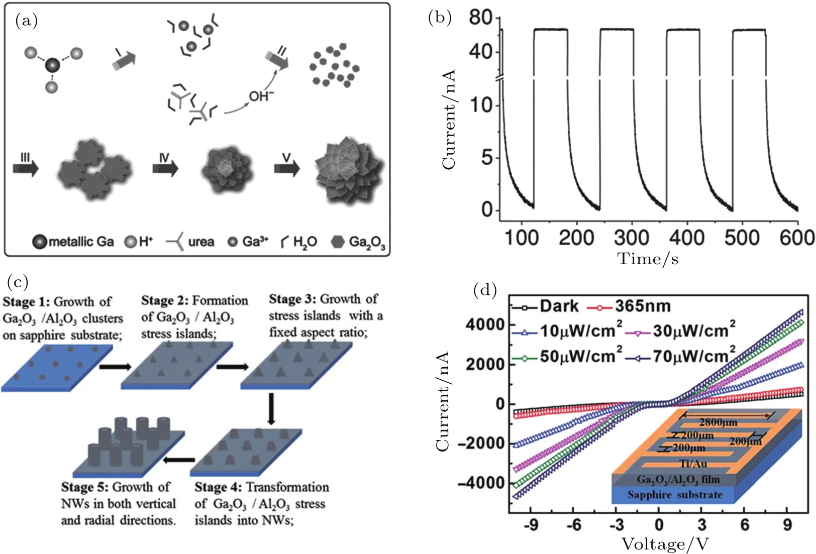
Fig.6.(a)Schematic illustration describing the formation and(b)current-time curve of the Ga2O3 nano flower and PD;[84](d)schematic diagram and(e)I-V curves of the photodetector based on Ga2O3 nanowires grown at 650°C.[46]
ZnGa2O4nanowire is a ternary oxide semiconductor that can be used as high-performance UV PDs.Lou et al.grew ZnGa2O4nanowires by a simple vapor transport method and fabricated MSM photodetector.The schematic of the device and SEM image of the nanowires are shown in Fig.7(a).A single nanowire was used as the channel layer for UV light detection.Figure 7(b)shows the time-dependent current curves at different bias voltages.The rise time and decay time were about 15 s and 10 s,respectively.The light current obviously increases as the bias voltage is improved.The results reveal that ZnGa2O4nanowires show good sensitivity to the UV light.
The different structures of PDs have their own advantages and disadvantages.The photodetection performance of the AlGaN-based PDs and Ga2O3-based PDs,including Schottky photodiode,MSM structure,PN junction,and APD structure,is summarized in Table 1.For the AlGaN-based PDs,the MSM structure has a simple frication process and mezzo responsivity.The Schottky barrier diode(SBD)and p-n junction PDs show very fast response time but low responsivity and detectivity.APD-based PDs are suitable for the weak signal detection because of its multiplication effect.For the Ga2O3-based PDs,MSM is the most used structure.The responsivity of the Ga2O3-based PDs with FET structure is much bigger than the other structures.
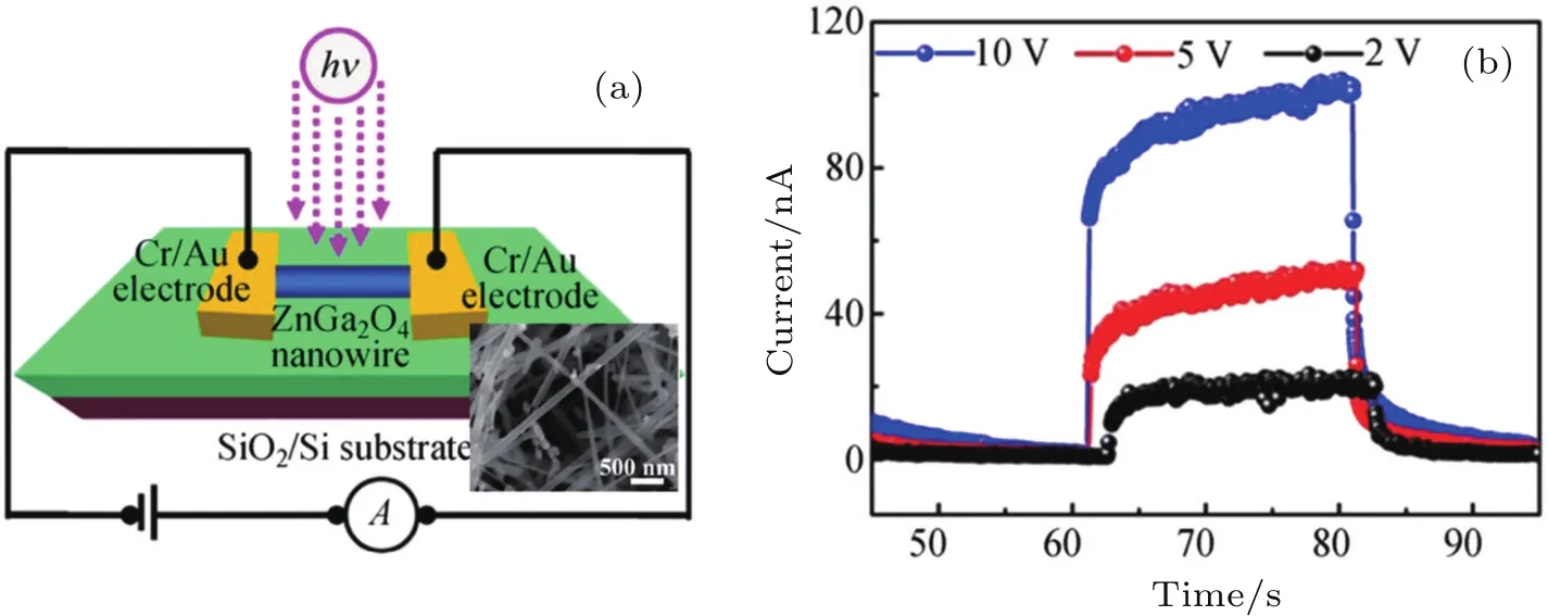
Fig.7.(a)Schematic diagram and(b)photoresponse characteristics of the photodetector on SiO2/Si substrate.[47]
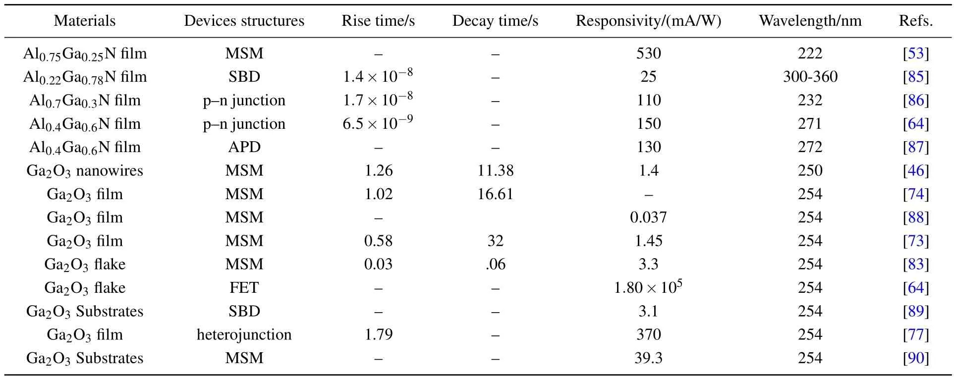
Table 1.Photodetection performance of the AlGaN-based and Ga2O3-based PDs.
4.Conclusions and outlook
We review the recent research progress in AlGaN-based and Ga2O3-based solar-blind UV photodetectors.The growth temperature ofAlNnucleation and middle-temperature ofAlN interlayer play important roles in the quality of the AlGaN film.The AlN cap layer can reduce the dark current while the recess structure is beneficial to the light current of AlGaN-based MSM PDs.High/low-Al-content AlGaN layer and grading AlGaN layer can improve the performance of AlGaN APD.The Ga2O3film grown by PLD,MBE,and MOCVD show good solar-blind UV photodetection capability.The Ga2O3flakes could be mechanically exfoliated from the single substrate and fabricated to MSM photodetector.Ga2O3nano flower and nanowires are also good solar-blind UV photodetectors.The APD structure of AlGaN-based PDs could detect very weak signals because of its multiplication effects.As to the Ga2O3-based PDs,the FET structure shows the highest responsivity and response speed.Although much progress has been made about Ga-based solar-blind photodetectors,there is still a lot of research work to further develop the performance of AlGaN and Ga2O3-based solar-blind photodetectors.The enhancements of crystallization quality and p-type doping concentration of the AlGaN layer are important to the AlGaN-based photodetector.At the same time,the growth technology and device structure of Ga2O3-based photodetector need further improvement.
猜你喜欢
杂志排行

Chinese Physics B的其它文章
- Superlubricity enabled dry transfer of non-encapsulated graphene∗
- Synthesis and characterization of β-Ga2O3@GaN nanowires∗
- Low-energy(40 keV)proton irradiation of YBa2Cu3O7-x thin films:Micro-Raman characterization and electrical transport properties∗
- Preliminary investigation on electrothermal instabilities in early phases of cylindrical foil implosions on primary test stand facility∗
- Effects of secondary electron emission on plasma characteristics in dual-frequency atmospheric pressure helium discharge by fluid modeling∗
- In fluence of low-temperature sul fidation on the structure of ZnS thin films∗