Transition of photoconductive and photovoltaic operation modes in amorphous Ga2O3-based solar-blind detectors tuned by oxygen vacancies∗
2019-02-25YanFangZhang张彦芳XuanHuChen陈选虎YangXu徐阳FangFangRen任芳芳ShuLinGu顾书林RongZhang张荣YouDouZheng郑有炓andJianDongYe叶建东
Yan-Fang Zhang(张彦芳),Xuan-Hu Chen(陈选虎),Yang Xu(徐阳),Fang-Fang Ren(任芳芳),3,Shu-Lin Gu(顾书林),3,Rong Zhang(张荣),3,You-Dou Zheng(郑有炓),3,and Jian-Dong Ye(叶建东),3,†
1 Jiangsu Provincial Key Laboratory of Advanced Photonic and Electronic Materials and School of Electronic Science and Engineering,Nanjing University,Nanjing 210093,China
2 Wuxi Institute of Technology,Wuxi 214121,China
3 Collaborative Innovation Center of Solid-State Lighting and Energy-Saving Electronics,Nanjing University,Nanjing 210093,China
Keywords:amorphous gallium oxide,solar-blind photodetector,photovoltaic,photoconductive
1.Introduction
Solar blind photodetectors find numerous applications in space communication,missile tracking, flame detection,ozone monitoring,and biological analysis.[1]As an ultra-wide bandgap semiconductor,Ga2O3is a promising candidate for solar-blind photodetectors due to its intrinsic solar-blindness with a desirable bandgap of about 4.8 eV.The advantages of a high breakdown field and a high resistance against radiation are expected to endow Ga2O3detectors with the strong capability to capture weak ultraviolet(UV)signals with low false alarm rates even operated in harsh environments.[2]To date,high performance β-Ga2O3based solar-blind photodetectors have been reported.[3-5]While most of them are based on β-Ga2O3bulk crystal,crystalline epilayers,or nanostructures which require high synthesis temperature and complicated processes,Cui et al.have recently reported a high-responsespeed solar blind photodetector on flexible substrates based on amorphous Ga2O3synthesized at room temperature.[6-8]Therefore,amorphous Ga2O3material has been proven as an alternative platform for delivering high performance solarblind detectors due to its unique advantages of thermal-budget synthesis on flexible substrates and easy fusion with modern high-speed integrated circuitry.[6]
Since there is no sign of achieving p-type Ga2O3,the most attractive Ga2O3-based photodetectors are constructed in Schottky-barriermetal-semiconductor-metal(MSM)architectures because of their figure-of-merits including low dark current,low capacitance,intrinsic high speed,and fabrication simplicity.However,most of the present Ga2O3detectors exhibit high gains while sacrificing the response speed,because they are operated in a mixing of photoconductive and photovoltaic modes.[8,9]The photoconductive detectors could only ensure the maximum presence of the intrinsic feature of absorbing layers,while the response time even lasts several hours due to the contribution of persistent photoconductivity(PPC)effect induced by oxygen vacancies in oxide semiconductors.[10,11]In the ideal Schottky-barrier photovoltaic detectors,carrier transport can be effectively manipulated by the built-in field,leading to a high efficient separation and collection of excess carriers with a fast speed.However,self-trapped holes in the vicinity of metal-semiconductor(MS)interface were reported to reduce the carrier emission barrier from traps,yielding high internal gains and degrading response speeds.[12]Therefore,carrier transport across MS interface normally controls the operation modes while the quality of absorbing layer and interface predominantly determines the device performance.For amorphous Ga2O3synthesized at a low temperature,insufficient oxygen incorporation inevitably introduces oxygen vacancies within the absorbing layer and in the vicinity of MS interface.[6,13]The correlation of carrier transport,defect behaviors,operation modes,and performance of photodetectors needs further understanding,which is crucial to design high performance solar-blind Ga2O3photodetectors towards practical applications.
In this work,we demonstrate the tunable conductivities of amorphous Ga2O3films by varying oxygen flux during the sputtering process,which consequently leads to the conversion of contact types and the transition of device operation modes.Interdigital MSM photoconductors with Ohmic contacts exhibit high internal gains but slow response speeds accompanied with an obvious sub-gap absorption,which results from the abundant deep-level traps and their associated PPC effect induced by oxygen vacancies.The oxygen incorporation effectively results in semi-insulating film and the resulting photovoltaic detector delivers superior performance with an ultralow dark leakage current,a high rejection ratio,suppressed sub-gap absorption,and a fast response speed.The correlation of carrier transport and device performance has also been discussed in details.
2.Experimental section
The 125-nm-thick Ga2O3thin films were deposited on sapphire(0001)substrate by radio frequency(RF)sputtering on a high purity(99.999%)Ga2O3ceramic target at room temperature(RT).During the growth,the RF power was maintained at 180 W with an argon flux of 40 sccm,and the growth pressure was 0.4 Pa.To distinguish the oxygen incorporation,two samples(denoted as S1 and S2)were grown without or with incorporating oxygen flux of 4 sccm,respectively,while other growth conditions were identical.Both the resultant films exhibit amorphous features with smooth surface morphology as determined by the x-ray diffraction patterns and atomic force microscopy(not shown here).Following standard lithography procedures,Ti/Au(40 nm/10 nm)metalstack was deposited using an e-beam evaporator to form MSM architectures,as shown in the inset of Fig.1(b),which consist of 25-pair fingers with 5 µm in width spaced by a 5-µm gap,and 440µm in length.
Transmittance spectra were measured at room temperature using a PerkinElmer Lambda 950 system with a sapphire substrate as the reference.The current-voltage(I-V)characteristics were performed using a Keithley source meter model 2636 A in dark or under illumination of 254-nm light(Model ENF-240C/FE)with an incident power density of 0.5 mW/cm2.The spectral photoresponse was measured using a monochromator(model iHR320)equipped with a 300-W xenon-arc lamp as the opticalexcitation source and a low noise current preamplifier(model SR570)with the lock-in measurement technique(model SR830).The incident power density was calibrated by a Si reference photodiode.A 266-nm pulsed laser with a single pulse energy of 2µJ was employed as the excitation source for temporal response measurements,and a digital oscilloscope(TBS 1102)for data collection.
3.Results and discussion
The incorporation of oxygen flux is expected to tune the sub-gap states which can be reflected by the optical transmittance spectra as shown in Fig.1(a).In comparison,the sample S2 grown with oxygen flux exhibits steeper absorption edge with a high transmittance,while an obvious absorption shoulder in the spectral range of 280 nm-400 nm is observed for sample S1,indicating the presence of sub-gap states.The optical bandgap and distribution of sub-gap states can be described by using Tauc and Urbach rules.[14,15]Approximated absorption coefficient α can obtained in terms of exp(-αd)=T/(1-R),where d is the film thickness,and T and R represent the transmittance and reflectance components,respectively.As plotted in the inset of Fig.1(a),the dependence of()2on ħν exhibits linear features and are well fitted by the Tauc relation offor direct semiconductors,where Egis the Tauc optical bandgap,is photon energy,and A2is the slope of absorption edges.[14]As summarized in Table 1,the optical bandgap is estimated to be 4.90 eV,in agreement with the reported value for the amorphous Ga2O3films.It is noted that the optical bandgap has no obvious change but a pronounced suppression of Urbach tail absorption below the bandgap is observed for sample S2 in the inset of Fig.1(a),indicating the reduction of sub-gap states with the incorporation of oxygen flux.It is well accepted that oxygen vacancies are the most dominant intrinsic defects,which are abundant and introduce broad band tails below the conduction band of amorphous and crystalline oxides if grown with insufficient oxygen incorporation.
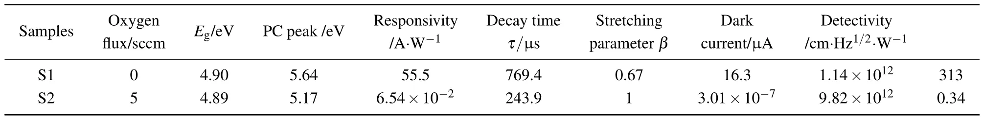
Table 1.The summary of the amorphous Ga2O3 photodetectors performance.
The variation ofsub-gap states below the conduction band also tunes the conductivities of the resultant films.Figure 1(b)shows the current-voltage(I-V)characteristics in dark condition.Without oxygen flux during the growth,the I-V curve shows a linear feature,indicating Ohmic contact of Ti/Au on the conductive Ga2O3layer,and the dark current at a bias of 5 V reaches 16.3µA.In contrast,an obvious rectifying behavior for back-to-back Schottky contacts with a very low dark current less than 1 pA is observed from the I-V characteristics of the sample S2.The asymmetric rectifying behavior is attributed to the inhomogeneous Schottky barriers.The conversion of metal-semiconductor contacts results from the conductivity variation of as-grown Ga2O3films tuned effectively by oxygen incorporation.It is well understood that insuf ficient oxygen incorporation will lead to the abundant oxygen vacancies distributed within the film,which will directly or indirectly donate electrons as donors and modify the conductivity.To understand the in fluence of oxygen vacancies on the carrier transport mechanisms,the schematic energy band diagrams of Ti/Ga2O3interface with Ohmic and Schottky types are shown in Figs.1(c)and 1(d),respectively.For conductive Ga2O3film,despite of the presence of Schottky barrier between Ti/Au and Ga2O3,the Fermi level of amorphous Ga2O3is pinned close to the energy levels of charged oxygen vacancies(),which is near the bottom of the conduction band.[16]Consequently,the barrier width becomes quite narrow,which allows easy passage of carrier via tunneling and thereby results in a good ohmic characteristic.Furthermore,as shown in Fig.1(c),traps under conduction band near the MS interface are also abundant and hence trap-assisted tunneling(TAT)wil also be promoted to increase the reverse current.[17]Oxygen flux incorporation effectively suppresses the formation of oxygen vacancies and donor-like surface traps,resulting in semi-insulating feature of the film and the reduction of interface states near the M-S contacts.In this case,the space charge region is broad enough to suppress the field-emission tunneling or trap-assisted tunneling processes,as shown in Fig.1(d).Thus,a very low dark current is expected in the back-to-back Schottky junction together with a high resistive Ga2O3layer in series.Apart from the injection-limited conduction mechanism,the bulk-limited conduction mechanism such as Ohmic conduction should also be taken into account to describe such low reverse current in the high resistive sample S2.[18]
The conversion of metal contacts to the amorphous Ga2O3layer gives rise to the resultant MSM photodetectors working in different operation modes with different photoresponsivity performance.Figure 2(a)shows the semi-log I-V plots of the photodetector in dark condition and under illumination of 254 nm deep ultraviolet(DUV)light.With oxygen incorporation,both dark current and photocurrent components decrease in 109and 104of magnitudes,respectively,mainly limited by the back-to-back Schottky contacts.As a result,a high photocurrent/dark ratio of 105is achieved,which demonstrates that low background noise with ultralow dark current will enhance the capability to detect weak UV signals.Figures 2(b)and 2(c)show the spectral dependence of absorption coefficient and photoresponsivity of photodetectors biased at 5 V,respectively,plotted in a semi-log scale.The difference in spectral photoresponse characteristics is attributed to the detectors working in photoconductive and photovoltaic modes for samples S1 and S2,respectively.The sample S1 has a peak responsivity of 55.5 A/W at 5.64 eV,yielding a high productofexternalquantum efficiencyηextand internalgain G of 313.[19]For the photoconductor S1,a rather low rejection ratio is obtained accompanied with a distinct and broad response tail down to 4.0 eV,which is very similar to the shape of sub-gap absorption in the absorption coefficient spectrum in Fig.2(b).The sub-gap absorption is known as the Urbach tail and follows an exponential dependence versus energy with a characteristic energy Eu,which depicts the density of states below the bandgap.Both the absorption coefficient and photoresponse below bandgap can be well described by similar relations ofandrespectively.[14,20]The Urbach tail states are originated from defects with their energy level close to the conduction band,and in this work,oxygen vacancies and gallium interstitials are the most possible candidates.It has been widely reported that donor like oxygen vacancies in the absorbing layer captures the excess photogenerated carriers under illumination,leading to serious PPC effect and yielding a high photoconductive gain.[6,10,11]
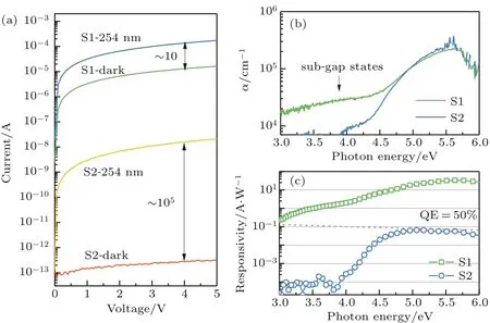
Fig.2.(a)Semi-log scaled I-V characteristics of detectors in dark condition and under illumination of 254 nm DUV light;(b)semi-log plots of absorption coefficients α versus hν;(c)semi-log plots of photoresponse versus hν for samples S1 and S2 measured at room temperature with a biase of 5 V.
In comparison,a peak responsivity of 0.065 A/W at 5.17 eV with a corresponding ηextG ≈ 50%is achieved for sample S2 with a sharp cutoff edge near the energy gap,and a high ultraviolet C(UVC)-to-ultraviolet A(UVA)rejection of about 103with suppressed sub-gap absorption.It is a sign that the sample S2 is operated in the typical photovoltaic mode with its ideal maximum internal gain to be unity,in which,excess electron-hole pairs generated in the depletion region are separated and driven by the built-in field,mainly contributing to the photocurrent.The thermal-noise-limited detectivity D∗,a figure of merit used to characterize the smallest detectable signal,is determined to be 1.14×1012cm·Hz1/2·W-1and 9.82 × 1012cm·Hz1/2·W-1for samples S1 and S2 biased at 5 V,respectively,in terms of the relation of D∗=RA1/2/(2qId)1/2,where R is the peak responsivity,A is the effective illumination area,q is the electronic charge,and Idis the dark current at the applied bias.[1,21]It can easily come to the conclusion that the photovoltaic detector with tremendous reduction of defects by oxygen incorporation demonstrates superior device performance as summarized in Table 1.Another interesting feature is that both response spectra are composed of two bands located at 5.64 eV and 5.17 eV as shown in Fig.3(a),which are consistent with the energy positions for the maximum of absorption coefficient in Fig.2(b)and the Tauc optical bandgap,respectively.It may be understood in the framework of valance band structure of Ga2O3that is mainly determined by oxygen 2p states.[2,22]Especially for the amorphous materials,the disorders lead to the relaxation of selection rules that are only valid for the transitions at the Γ point in single crystalline materials.As a matter of fact,the optical transitions are not restricted at Γ point but are allowed in the whole Brillouin zone,and thus,transitions from deeper valance sub-bands to the conduction bands are dominant in sample S1,leading to the blue-shift of peak responsivity.
Fig.3.(a)Frequency-dependent photoresponsivity spectra under the bias of 5 V;(b)the dependence of peak responsivity on the chopping frequency and the fitting of effective lifetime of excess carriers in samples S1 and S2;(c)temporal response characteristics of the photodetectors illuminated by a 266-nm pulse laser at 5-V bias and the fitting plots by a stretched exponential function.
The devices operated in photoconductive and photovoltaic modes are also expected to have different transient photoresponse characteristics.Figure 3(a)shows the spectral photoresponsivity of devices recorded at different chopper frequencies.Apparently,as the chopping frequencies increase,the magnitude of peak responsivity for sample S1 decreases much quicker with respect to that of sample S2.The dependence of peak responsivity on the modulation frequency is extracted in Fig.3(b).The effective lifetime of excess carriers can be determined by the relation of R=Aτeff/?1+ω2τeff?1/2,where A is the function of intrinsic carrier concentration,quantum efficiency,detection wavelength,and applied bias.[1]The good fitting to the solid experimental points in Fig.3(b)gives rise to a carrier lifetime of 23 ms and 2.3 ms for samples S1 and S2,respectively.Finally,the temporal photoresponse was measured with 5-V bias under illumination of a 266-nm pulsed laser.The decay curves can be well described by a stretched exponential function of,where τ is the response decay time,andβ isthe stretching parameterbounded between 0 and 1.[23]The variation of β from unity is a measure for the degree of disorder in the material and has been widely used to describe the decay processes involved in the localized centers such as InGaN,[24]II-VI quantum dots,[25]and porous Si.[26]The good fitting in Fig.3(c)gives rise to the decay times of 769.4 µs and 243.9 µs as well as the β values of 0.67 and 1.0 for samples S1 and S2,respectively.The increased β value in S2,together with sharp edges of absorption and photoresponse,indicates the decreased trap densities by oxygen incorporation.It is noted that the extracted decay time in Fig.3(c)is much shorter than the response time determined by chopper-modulated Xe-lamp light due to its low incident light power.The excitation-dependent response could be attributed to the redistribution of the excess carriers with increased excitation level,which are also observed in the photoconductive detectors fabricated from wide bandgap materials.[21]Nevertheless,the different photoresponse characteristics of two devices operated at different modes are strongly linked to the carrier transport mechanisms,including electron-hole generation,trapping,and recombination.It is expected that the transport time of excess carriers driven by built-in field in the depletion region for the photovoltaic detector is much shorter than the transition time of carriers between two interdigital fingers of photoconductors.In particular,with the presence of abundant oxygen vacancies,trapping of photogenerated holes slows the recombination process and thus leads to long decay time.Oxygen incorporation in the growth process is essential to reduce deep-level traps,and therefore the photogenerated electrons and holes undergo a rapid separation and combination process,promoting a fast response recovery.To improve the photodetector performance,some further strategies are required,including improving the carrier mobility to reduce the carrier transit time,[1]reducing the deeplevel trapping of minority carriers to suppress the persistentphotoconductivity effect,[27]surface passivation to reduce surface recombination,[28]or inducing additional built-in field by using novel designs of heterostructure[5,29]or three-terminal phototransistors.[30]
4.Conclusions
In conclusion,an Ohmic-type phtoconductive and a Schottky-type photovoltaic photodetectors based on amor-phous Ga2O3film have been fabricated by tuning the oxygen flux during the sputtering process.The conversion of contact types and the operation mode transition of photodetectors are attributed to the variation of oxygen vacancy concentration in Ga2O3films.Oxygen incorporation tremendously reduces the oxygen vacancies within the absorbing layer and interface states at the metal-semiconductor contacts,which suppresses the sub-bandgap absorption and persistent photoconduction effect.Consequently,the Schottky photovoltaic detector shows superior performance with an ultra-low dark current at pA level,a high detectivity of 9.82×1012cm·Hz1/2·W-1,a fast response time of 243.9µs,and a high UVC-to-UVA rejection ratio of 103.The results provide a paradigm for the realization of high performance and cost-effective amorphous Ga2O3based solar blind photodetectors with broad applications.
Acknowledgment
We would like to thank Prof.Yi Yang and A/Prof.Dongming Tang to provide the sputtering system for the synthesis of Ga2O3materials.
猜你喜欢
——江苏邳州老年大学校歌
杂志排行

Chinese Physics B的其它文章
- Superlubricity enabled dry transfer of non-encapsulated graphene∗
- Synthesis and characterization of β-Ga2O3@GaN nanowires∗
- Low-energy(40 keV)proton irradiation of YBa2Cu3O7-x thin films:Micro-Raman characterization and electrical transport properties∗
- Preliminary investigation on electrothermal instabilities in early phases of cylindrical foil implosions on primary test stand facility∗
- Effects of secondary electron emission on plasma characteristics in dual-frequency atmospheric pressure helium discharge by fluid modeling∗
- In fluence of low-temperature sul fidation on the structure of ZnS thin films∗