High Sensitivity Hall Devices with AlSb/InAs Quantum Well Structure
2017-12-05-,-,-,-
-, -, -, -
(School of Electronic Engineering, Xi’an University of Posts and Telecommunications, Xi’an 710121, China)
HighSensitivityHallDeviceswithAlSb/InAsQuantumWellStructure
WULi-fan*,MIAORui-xia,LIYong-feng,YANGXiao-feng
(SchoolofElectronicEngineering,Xi’anUniversityofPostsandTelecommunications,Xi’an710121,China)
An unintentionally doped AlSb/InAs quantum well (QW) structure and a Si-δ doped quantum well structure on GaAs (001) substrates were grown by molecular beam epitaxy (MBE). The dependence of sheet electron density and electron mobility on the measurement temperature were investigated. It is found that electron mobility as high as25000cm2·V-1·s-1has been achieved for300K in the Si-δ doped quantum well structure. The Hall devices with high sensitivity and good temperature stability were fabricated based on the Si-δ doped AlSb/InAs quantum well structures. Their sensitivity is markedly superior to Hall devices of an unintentionally doped AlSb/InAs quantum well.
Hall device; quantum well; δ-doping; molecular beam epitaxy
1 Introduction
The Hall devices work on the principle of the classical Hall effects. They have been widely studied for the applications in magnetic sensors after the first generation of Hall magnetic sensors was fabricated in the mid-1950s[1-2]. The sensors have been developing quickly along with the progress of material growth technology, such as molecular beam epitaxy (MBE) and metal-organic chemical vapor deposition (MOCVD). In addition, a large conduction band discontinuity between InAs and AlSb (ΔEc=1.35 eV) provides the deepest quantum wells available for any other lattice-matchedⅢ-Ⅴ heterostructure[3], by virtue of the InAs material high electron mobility (30 000 cm2·V-1·s-1at 300 K) and high electron velocity (4×107cm·s-1)[4]. However, there are still many challenges to obtain high sensitivity Hall devices. On the one hand, by the lack of zincblende insulating substrates with lattice constant matched to InAs and AlSb alloys[5-8]. On the other hand, some other issues, such as the design of proper band structure, the increase of two dimensional electron gas (2DEG) densities, mobility should also be addressed. In this paper, we grow the unintentionally doped quantum well structure sample and the single Si-δ doped quantum well structure sample by MBE technology. Moreover, the influence of the measurement temperature on the sheet electron density and electron mobility are investigated. Finally, Hall devices are manufactured with excellent performance.
2 Experiments
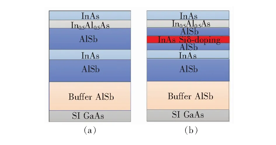
In this work, two different Hall devices were prepared: an unintentionally doped quantum well structure sample and a Si-δ doped quantum well structure sample. The schematic structures of two samples are shown in Fig.1. All these two samples in this work were grown on semi-insulating GaAs (100) substrates by VG80-H molecular beam epitaxy (MBE) system.In-situreection high-energy electron diffraction (RHEED) was employed to observe the surface reconstruction as well as to monitor the growth rates.
For sample A1, a 1.2 μm relaxed metamorphic AlSb buffer layer wasrstly deposited at 550 ℃, in order to accommodate about 7% compressive lattice mismatch between the GaAs substrate and the InAs channel[9-11].“In-Sb like” is formed at the InAs/AlSb interfaces to offer the best transport characteristics in the InAs channel[8].
Sample A2 includes a Si-δ doped epitaxial layer compared with sample A1. The Si δ-doping plane in 1.2 nm InAs is inserted in AlSb layer. The material structure is shown in Fig.1. The Hall devices with Ti/Pt/Au Ohmic electrodes, deposited by an e-beam evaporator, were fabricated by wet-etching. Finally, Si3N4was deposited with as a passivation layer.

Fig.1 Schematic structure of Hall devices epitaxial layers. (a) Sample A1, unintentionally doped. (b) Sample A2, a Si-δ doped.
3 Results and Discussion
All samples were grown by VG80-H MBE system. Atomic force microscopy (AFM) is applied to characterize the surface morphology using a contact mode. The electron mobility and sheet electron density were measured by van der Pauw Hall measurements, in which the temperature range is from 300 to 77 K to investigate the change of sheet electron density with temperature.
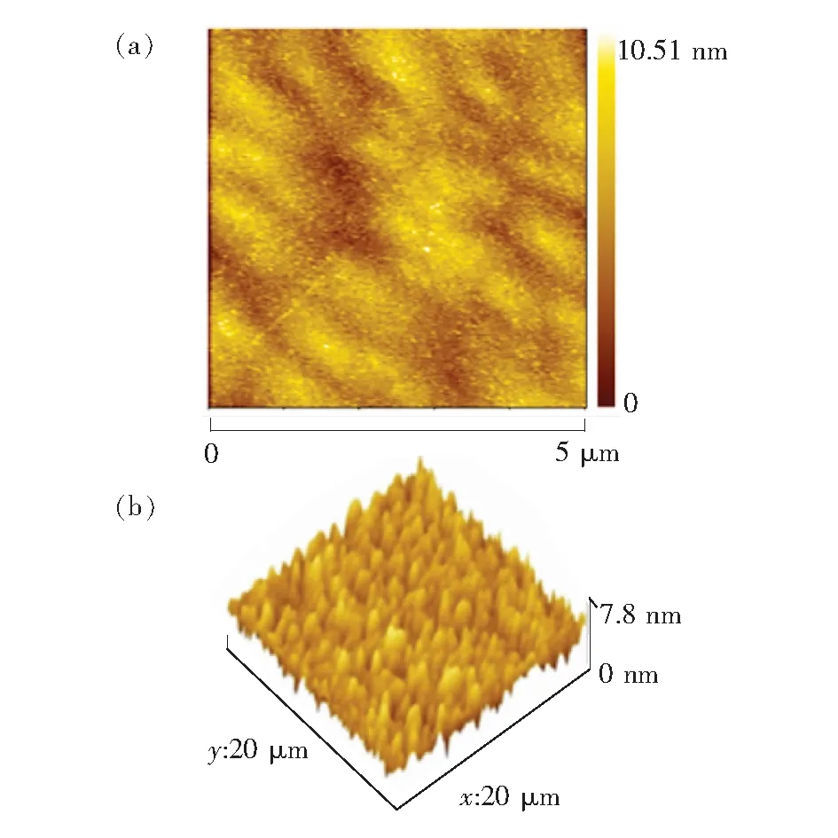
Fig.2 shows the 2 μm×2 μm AFM micrograph of sample A2. The surface root-mean-square roughness and peak-to-valley height are 0.68 and 7.8 nm respectively, indicating a smooth surface morphology.

Fig.2 2 μm×2 μm AFM micrograph of sample A2. (a) Two-dimensional. (b) Three-dimensional.
As can be seen from Fig.2, mounds with spiral steps but without obvious anisotropy were found on the surface.
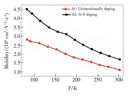
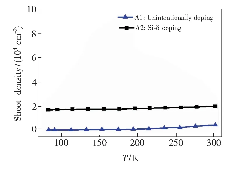
Hall measurements were performed from 77 to 300 K on two samples. Fig.3 shows the measured electron mobility from 77 to 300 K as a function of different measurement temperatures. As can be seen from Fig.3, two distinct temperature dependences of electron mobility can be observed. From 300 to 175 K, the electron mobilityvs. temperature for the structures of A1,A2 show identical variation trend and acoustic phonon scattering is the dominant scattering. However, in the temperature lower than about 175 K, the variation trends split and show obvious difference. At low temperature, the acousticphonon scattering is weakened because of the weak vibration of atoms. In Fig.4, the sheet electron densities of these two samples are shown with measurement temperature from 300 to 77 K. As can be seen from the figure, the sheet electron density keeps almost constant for the samples in different temperatures and becomes less temperature dependent. However, the sheet electron density of the sample A2 is higher than sample A1.

Fig.3 Electron mobilityvs. temperature for sample A1 and A2

Fig.4 Temperature dependence of sheet electron concentration of sample A1 and A2
Tab.1 shows the characteristics of two types of Hall devices, such as the mobility, input resistance, output resistance, and sensitivity. As the table shows, the room-temperature sensitivity of 108 mV·mA-1·kG-1·kΩ-1was achieved for the Hall devices based on the Si-δ doped AlSb/InAs quantum well structure sample, which is almost twice as sensitive as the devices based on the unintentionally doped quantum well structure. The high mobility of the Si-δ doped AlSb/InAs quantum well structure is advantageous to the high sensitivity for Hall devices. The higher sheet carrier concentration can improve the operation sensitivity. Thus, by optimizing the δ-doping and 2DEG structure design, we can obtain high mobility and sheet density and good sensitivity simultaneously.

Tab.1 Characteristics of two samples of Hall devices
4 Conclusion
In summary, an unintentionally doped AlSb/InAs quantum well structure and a Si-δ doped quantum well structure on GaAs (001) substrates were grown by molecular beam epitaxy (MBE), and according to these, Hall devices were fabricated. The performance of Hall devices based on the Si-δ doped AlSb/InAs quantum well structures have been significantly improved, compared with that of an unintentionally doped AlSb/InAs quantum well devices.
[1] ZHANG Y, ZHANG Y W, WANG C Y,etal.. High sensitivity Hall devices with AlSb/InAs quantum well structures [J].Chin.Phys. B, 2013, 22(5):057106-1-3.
[2] DINGLE R, STORMER H L, GOSSARD A C,etal.. Electron mobilities in modulation-doped semiconductor heterojunction superlattices [J].Appl.Phys.Lett., 1978, 33(7):665-667.
[3] BENNETT B R, MAGNO R, BOOS J B,etal.. Antimonide-based compound semiconductors for electronic devices: a review [J].Solid-StateElectronics, 2005, 49(12):1875-1895.
[4] TUTTLE G, KROEMER H, ENGLISH J H. Effects of interface layer sequencing on the transport properties of InAs/AlSb quantum wells: evidence for antisite donors at the InAs/AlSb interface [J].J.Appl.Phys., 1990, 67(6):3032-3040.
[5] 朱彦旭, 王岳华, 宋会会, 等. 基于GaN基HEMT结构的传感器件研究进展 [J]. 发光学报, 2016, 37(12):1545-1553.
ZHU Y X, WANG Y H, SONG H H,etal.. Progress of sensor elements based on GaN HEMT structure [J].Chin.J.Lumin., 2016, 37(12):1545-1553. ( in Chinese)
[6] WU L F, ZHANG Y M, LV H L,etal.. Atomic-layer-deposited Al2O3and HfO2on InAlAs: a comparative study of interfacial and electrical characteristics [J].Chin.Phys. B, 2016, 25(10):108101-1-5.
[7] MAHER H, BOLOG C R, PINER E L. High-transconductance delta-doped InAs/AlSb HFETs with ultrathin silicon-doped InAs quantum well donor layer [J].IEEEElectronDev.Lett., 1998, 19(3):83-85.
[8] WANG J, XING J L, WEI X,etal.. Investigation of high hole mobility In0.41Ga0.59Sb/Al0.91Ga0.09Sb quantum well structures grown by molecular beam epitaxy [J].Appl.Phys.Lett., 2014, 104(5):052111-1-5.
[9] TANG J S, YU G Q, WANG C Y,etal.. Versatile fabrication of self-aligned nanoscale Hall devices using nanowire masks [J].NanoLett., 2016, 16(5):3109-3115.
[10] WANG K, HUANG Y, QIU Y Z,etal.. Magnetic properties of ultrathin CO/Pt multilayer Hall devices irradiated using focused ion beam [J].PhysicaB:CondensedMatter, 2015, 476(1):158-160.
[11] CHEN D, ZHAO B Q, ZHANG X. High signal-to-noise ratio Hall devices with a 2D structure of dual δ-doped GaAs/AlGaAs for low field magnetometry [J].Chin.Phys.Lett., 2015, 32(12):128502-128506.
高灵敏度InAs/AlSb量子阱的霍尔器件
武利翻*, 苗瑞霞, 李永峰, 杨小峰
(西安邮电大学 电子工程学院, 陕西 西安 710121)
用分子束外延在GaAs (001)衬底上生长了两个量子阱结构的霍尔器件,一个是没有掺杂的量子阱结构,一个是Si-δ掺杂的量子阱结构。研究了霍尔器件的面电子浓度和电子迁移率与温度的关系。结果表明,在300 K下,Si-δ掺杂的量子阱结构的电子迁移率高达25 000 cm2·V-1·s-1,并且该器件输入电阻和输出电阻较低。同时,Si-δ掺杂的量子阱结构霍尔器件的敏感度好于没有掺杂的量子阱结构霍尔器件。
霍尔器件; 量子阱; δ掺杂; 分子束外延
2017-05-05;
2017-09-30
国家自然科学基金青年基金(51302215); 陕西省教育厅科研计划(17JK0698)资助项目
1000-7032(2017)12-1650-04
*CorrespondingAuthor,E-mail:wulf0608@163.com
TN305; TN382DocumentcodeA
10.3788/fgxb20173812.1650
Supported by National Natural Science Foundation of China (51302215); Scientific Research Program Funded by Shaanxi Provincial Education Department (17JK0698)

武利翻(1980-),女,山西忻州人,博士研究生,讲师,2006年于重庆邮电大学获得硕士学位,主要从事Ⅲ-Ⅴ族HEMT、传感器等半导体器件的研究。E-mail: wulf0608@163.com
