光电催化分解水的光阳极改性策略
2017-03-13邱伟涛黄勇潮王子龙纪红兵童叶翔
邱伟涛 黄勇潮 王子龙 肖 爽 纪红兵,* 童叶翔,*
(1中山大学化学学院,广州510275;2香港科技大学化学系,香港999077)
光电催化分解水的光阳极改性策略
邱伟涛1黄勇潮1王子龙2肖 爽2纪红兵1,*童叶翔1,*
(1中山大学化学学院,广州510275;2香港科技大学化学系,香港999077)
光电催化分解水系统能直接将收集的电子与空穴用于分解水,将太阳能转化成了具有高能量密度的氢气,是一种集太阳能转化和储存于一体的高效绿色能源系统。光阴极和光阳极串联要求其在工作状态下两电极通过的总电流必须一致,低效率的一端将会限制整个体系的反应速度,因此对于光阳极材料的系统研究具有十分重要的意义。理论预测表明,基于部分可见光响应的半导体光阳极能带间隙计算得到的极限太阳能制氢转化效率达到了15%。但实际上由于光催化的整个过程是一个多步反应,各个步骤上发生的光生载流子的复合和损失导致了目前合成的相关电极材料的转换效率远低于理论水平。一般可以认为光催化过程包括五个步骤:光电极材料中电子的光致激发而产生电子-空穴对、电子和空穴由于能带弯曲的反向分离和传递、电子(或空穴)通过半导体-电解液界面的注入水中析氢(或析氧)、载流子的复合以及反应物和产物的传质过程。由于这些过程的进行效率与电极材料的本质特性和性能密切相关,为了评估材料性能而引入的一些效率指标往往和这几个步骤相对应。本文首先简要介绍了评价光阳极的一些效率计算以及它们与上述各个步骤的内在联系。最后,在前人和最近的研究基础上总结了几种对光阳极材料的主要提升策略,包括形貌控制、元素掺杂、异(同)质结和表面修饰等改性方法,对这些改性方法和各步骤效率之间的联系作了简单的介绍。
光电催化;分解水;光阳极;光催化步骤;改性策略

QIU Wei-Tao,received his BS degree in chemistry from Sun Yat-Sen University in 2014.He is currently a 2nd year master of physical chemistry student in Prof.TONGYe-Xiang′s group at Sun Yat-Sen University.His research focuses on the development of nanostructured materials and their application in energy conversion/storage fields like photo-electrochemical water splitting and lithium-ion batteries.

HUANG Yong-Chao,obtained his BS degree in Chemistry from Huizhou University in 2011 and MS degree from Jinan University in 2013.He received his PhD in School of Chemistry and Chemical Engineering of Sun Yat-Sen University in 2016.His research interests focuses on fabrication of functional nanostructures for applications in environment,such as photo-electrochemical/photo-catalytic water splitting,industrial wastewater and volatile organic compounds treatment.

WANG Zi-Long,received his BS(2010)and MS(2012)in the School of Chemistry and Chemical Engineering from Sun Yat-Sen University in China.He is currently a PhD candidate in Prof.YANG Shi-He′s group in the Department of Chemistry of the Hong Kong University of Science and Technology. His current research focuses on nano-materials and their applications for energy storage and fuel cells.

XIAO Shuang,received his BS degree (2012)in School of Physics from Huazhong University of Science and Technology in China.He is currently a PhD candidate in Professor YANG Shi-He′s group in Department of Chemistry from the Hong Kong University of Science and Technology. His current research focuses on perovskite solar cells,photoelectrochemical cells and catalysts.

JI Hong-Bing,is currently a professor in School of Chemistry and Chemical Engineering at Sun Yat-Sen University.He received his PhD in the Department of Chemical Engineering from South China University of Technology in 1997.After completing his PhD,he was a lecturer(1997), associate professor(2003)and professor (2006)at South China University of Technology.He carried out his postdoctoral research at Osaka University in Japan from2000-2002.His research focuses on catalysis and electrochemistry.

TONG Ye-Xiang,received his BS degeree in General Chemistry in 1985,MS in Physical Chemistry in 1988,and PhD in Organic Chemistry in 1999 from Sun Yat-Sen University.He is a professor of Chemistry in SchoolofChemistry atSun Yat-Sen University.His current research focuses on the electrochemical synthesis of alloys, intermetallic compounds and metal oxide nanomaterials,and investigation of their applications for energy conversion and storage.
1 Introduction
How to utilize solar energy with least cost has always been an open question left to be answered by one generation of researcher over another.So massive the quantity of incident power from thesun(1.3×10⁵TW),it well exceeds the total energy consumption on the earth and no doubt the conversion of solar energy to applicable form of energy will alleviate the situation of energy crises and accompanying environmental issues1.So far,the most direct method to transform solar energy artificially is to convert them straightforward into electricity,using devices known as photovoltaic cells(PVs)with the help of materials that are able to generate photovoltage upon illumination.This photo-generated voltage drop across a material serves as an instant driving force that“pump”electrons through outer circuit and exhausts upon the retrieval of light source,which render this system only able to harvest energy and yet to store them.As an alternative,direct conversion of solar energy into hydrogen(a chemical media for solar energy storage)in a photoelectrochemical cell(PEC),has been extensively studied since 1970s,when the solar assisted water oxidation is discovered at surface of TiO22-6.
Similar to photovoltaic cell,the driving force for solar-assisted water oxidation comes from the photovoltage generated by incident photon.At non-biased condition,band gap energy(Eg)of a semiconductor is a crucial factor that determines whether the water splitting process can successfully undergo at semiconductorelectrolyte interface.As shown in Fig.1 as an example in the oxygen generating side in PEC,electrons are excited by photons in light-accessible area with energy greater than Eg.This results in a split of quasi-Fermi levels of acceptor and donor,whose difference is normally regarded as photo-generated voltage(Vph). In experiments,this voltage can be measured through calculating the difference between open circuit potentials of the same electrode under illumination and in dark7-9.The measured Vphis normally less than Egof the semiconductor,due to the loss caused by factors like non-radiative recombination and non-ideal band structure in the photocatalytic system.This is why some semiconductors possess suitable band gap while remain incapable of achieving efficient water splitting reaction10.To proceed to oxidize water,there are several more processes to take place in the semiconductor,as displayed in Fig.1 as well.Besides light harvesting and photo-generation of carriers,the holes will migrate to the semiconductor-electrolyte interface and electrons in an opposite direction due to the upward band bending in an n-type semiconductor for water oxidation.After that,holes reach at surface will be injected into electrolyte for oxygen evolution reaction(OER)and electrons travel to counter electrode for hydrogen evolution reaction(HER).During the migration of carriers, chances are there the holes and electrons might recombine in certain spots.Therefore,the overall photocatalytic water splitting can be summarized into five steps:(a)light absorption,(b)charge transfer,(c)redox reaction or carrier injection,(d)adsorption, desorption,and mass diffusion of chemical species,and(e)charge recombination.Accordingly,the challenges in developing highperformance PEC lie in the unfavorable properties that counteract on those procedures.This review will give a brief introduction on evaluating efficacy of a PEC and main discussion on the strategies that researches have exploited to boost the performance of photoelectrode and hence the overall efficiency of a PEC system. Generally speaking,these strategies include nanostructuring11-14, doping15-18,building junctions19-21,and surface engineering22-25, strategies that shorten carrier migration path,improve transport efficiency,adjust band gap width,boost charge separation,and augment charge injection efficiencies.Cases concerning the implementation of the strategies are introduced as well.
2 Crucial parameters for evaluating a PEC system
In the study of a PEC photoelectrode,the most direct and explicit characteristic is the photocurrent density in photocurrent density-potential(J-V)curves.In fact,using only photocurrent density to evaluate a photosystem is far from comprehensive to understand the detailed events in the whole photocatalytic process. This section will give a brief explanation of several most used parameters as they will be involved in the later discussion of strategies implemented to improve photoelectrochemical performance.Some of the parameters,like transport efficiency (ηtransport)will be referred to as terms like bulk efficiency(ηbulk)or separation efficiency(ηsep),due to the different manner of expression from varied cited articles.In situation when it is necessary to clarify the concept,explanation will be added to clarify the concept in brackets following.For instance,if some authors were referring to transport efficiency using terms like bulk efficiency, ηtransportin brackets will be added after it as reminder.
2.1 Solar-to-hydrogen efficiency
Solar-to-hydrogen efficiency(STH)is the most important parameters in evaluating the actual efficiency of a PEC system.The definitions of solar to hydrogen efficiency is the ratio of chemical energy produced to the input solar energy at non-biased condition. This measure of efficiency reveals the loss of solar energy during photolysis process.The measurement of hydrogen amount generated at zero-bias is required,thus a direct quantification of hydrogen product through gas chromatography is recommended. Nonetheless,a measure of hydrogen based on current density isalso acceptable.The expression of STH is written as follows8,9:
STH=237000v/(P·S)=1.23Jsc·ηF/P
where,v represents hydrogen generation rate(mmol·s-1),P stands for input solar power(mW·cm-2),and S represents the geometric area of the electrode(cm2).To calculate STH using photocurrent, short circuit current(Jsc/(mA·cm-2))at zero-bias is required. Multiplying Jscwith 1.23 V,which is the voltage calculated based on the Gibbs free energy for water splitting reaction26,gives the total electrical power in the system.Faradic efficiency(ηF)here is used to give the actual power for hydrogen generation.
In order to achieve a high STH in PEC system,the electrode materials should absorb as much light in solar spectrum as possible,which requires the semiconductor having a band gap just narrow enough to absorb light with a wide range of wavelength and meanwhile not too narrow to produce sufficient photovoltage to drive on water splitting.With this consideration,suitable Egshould be important for achieving high STH efficiency.Fig.2 shows a plot of theoretical maximum photocurrent and STH as functions of Eg.Anatase TiO2with Egof 3.2 eV reaches only the 1%STH efficiency limit in ideal consideration,while hematite Fe2O3with Egof 2.1 eV could give a STH efficiency as much as 15%.High STH as hematite can produce,current research has yet achieved that value due to factors like the recombination issues in photocatalytic reaction process.Some other parameters to describe them and to evaluate PEC system are introduced,to further quantify the efficiency of different steps in PEC water splitting.
2.2 Light conversion and incident/absorbed photonto-current efficiency
To evaluate the light conversion ability of the photoelectrode at every single wavelength,two measures of efficiency were brought out:incident photon-to-current efficiency(IPCE)and absorbed photon-to-current efficiency(APCE).Different from the singlevalued STH efficiency,these two efficiency measures reveal the distribution of light conversion efficiency as functions of wavelength.IPCE can be written as follows:
IPCE(λ)=1240Jph/Pλ·λ
where,Pλis the incident power of light at certain wavelength λ, while Jphstands for the steady-state photocurrent per square centimeter under illumination with the same wavelength.By the look of the equation,one can find out that the definition of IPCE is exactly the ratio of converted electron/hole flux to the incident photon flux at a defined wavelength.As for APCE,the light harvesting efficiency(ηLHE)is considered and hence this efficiency is more helpful in discussion of intrinsic nature of a material.By taking ηLHEinto the consideration of photon flux calculation,which means to multiply Pλwith ηLHE,APCE can be expressed as IPCE dived by ηLHEas follows:
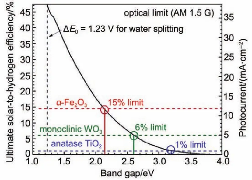
Fig.2 Ultimate photocurrent density and corresponding maximum STH of some semiconductors8
APCE(λ)=IPCE(λ)/ηLHE(λ)
In the above definition,the ηLHEequals to the ratio of absorbed photon flux to the total incident photon flux,expressed as27:
ηLHE(λ)=1-T(λ)=1-e-A(λ)
where,T represents transmittance of incident light with various wavelength,while A stands for absorbance of the sample.One should note that these two efficiencies are obtained from photocurrent at certain bias,which means that the values of IPCE and ABPE will vary according to the bias applied.Therefore,it is commonly recommended to be explicit in the bias used for these measurements.In many publications,electrode potential at 1.23 V(vs RHE(reversible hydrogen electrode))is usually used for acquisition of these two efficiencies.
2.3 Characteristics of J-V curves and relating efficiencies calculations
As we discussed the general procedures that take place in the complete water oxidation process,the photocurrent in a J-V curve of a typical photoanode can be expressed as28-31:
Jph=Jabs·ηtransport·ηinject
In the equation,Jabsrepresents the maximal photocurrent density a photoanode can achieve,taking the absorbed photons into account and assuming 100%ofAPCE all over the wavelength region with energy less than its Eg.This value can be calculated by integrating absorbed photon flux in a proper region.For hematite, this region is where photon energy is less than 2.1 eV,as shown in Fig.3(a).Absorbed photon flux is obtained by multiplying solar photon flux with ηLHEat each wavelength.Therefore,Jabsis in fact dependent on Egand ηLHE,an efficiency definition originated from the electrode absorbance in UV-Vis spectrum.As to quantify the charge separation and transport process in the bulk and interface, ηtransportand ηinjectare used.These values will not reach 100%in most cases since recombinations that take place both in bulk and interfaces will accordingly account for their loss in non-ideal condition28,30.As an example to demonstrate general way to obtain ηtransportand ηinject,typical J-V characteristics of photoanode for water oxidation with and without the addition of hole scavenger was displayed in Fig.3(b).In the presence of hole scavenger,an additive susceptible to oxidation,the kinetics barriers in oxidation process can be neglected.In this context,ηinjectis assumed to be 100%and thus the measured current Jscavis only limited by ηLHEand η27: transport
Jscav=Jabs×ηtransport
Hence,ηtransportequals to Jscavdivided by Jabswhile ηinjectat certain potential can be obtained from the ratio of Jscavto Jph,as shown in the figure.The two efficiency measures respectively describe thebulk events and surface events,both useful in evaluating the contribution from bulk separation and surface injection32.
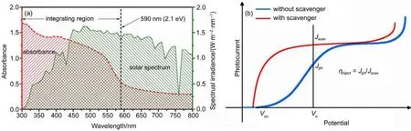
Fig.3 Solar spectrum,UV-Vis spectrum of hematite and typical J-V curves for photoanode
3 Strategies toward advanced PEC photoanode
In practical studies of PEC photoelectrode,the performance of a photoanode is restricted by the poor light harvesting ability of a semiconductor(e.g.improper Eg),poor mobility of photogenerated carriers(e.g.short diffusion length)and sluggish surface kinetics(e.g.unfavorable surface chemistry).These obstacles are effectively erased or attenuated by corresponding acting strategies: (a)nanostructuring or morphology manipulation that provides a most straightforward approach to reduce the requested minimal diffusion length to surface33-36and even serve as light trapping structure to make the best use of incident light within a relatively small film thickness37,38;(b)doping that modifies the intrinsic electronic structures to alter bulk properties like Egand conductivity of carrier39-42;(c)building hetero/homojunctions to enhance separation efficiency and broaden absorption spectrum of photoelectrode43-46;(d)loading of electro-catalyst or coating of surfacestate passivating layer that provides a faster reaction or thermodynamically more favored charge transfer through surface27,47-49; As a matter of fact,apart from cases we are going to introduce, there are thousands more examples left to be disclosed,whereas passage length is limited and only some cases we think representative are discussed.
3.1 Nanostructuring and morphology control
The variety of synthesis method and the complication in nanocrystal formation under varied conditions provides a large flexibility for photoanode nanostructuring.To date,special morphologies,such as nano-rods/wires50-53,nano-flakes54-56,nanotubes57-61,and nano-porous structures32,62,have been successfully fabricated.With reduced dimension of material geometry,nanorods and nano-flakes not only possess accessible area for the electrolyte contact,but also provide a short-cut for charge transport process,increasing ηtransportof an electrode40,63-65.
3.1.1 Nanostructure requiring shorter diffusion length
As shown in Fig.4(a-e),different representative morphologies are demonstrated.One of the commonest one-dimensional morphologies for hematite is shown in Fig.4(a)66,the diameter of the rod is narrowed down to nanometer scale,which drastically increases its charge separation efficiency and electron collection ability.Other than shortened distance for photo-generated carriers to reach surface,the electronic structure is rectified by a confinement effect known to exist in many miniaturized materials.In their studies of X-ray absorption spectrum(XAS)and resonant inelastic X-ray scattering,Vayssieres et al.66discovered that the band gap energy was widened due to the confinement effect, making them possible for non-biased full cleavage of water.Fig.4 (b)gives a representative example for two dimensional structures in PEC application.WO3nano-flakes grown on conductive substrate as active material,with typically thin sheets(30 nm)of metal oxides undoubtedly facilitating charge transferring process. No quantum confinement effect is pointed out for the material and the current density of the material reaches to~0.6 mA·cm-2at 1.23 V(vs RHE),outperforming many WO3photoanodes at the time.Other examples created porosity in TiO267and BiVO462.They both display pores for electrolyte infiltration to the inner space of the electrode while thin wall or small particle size can promote hole injection as well as electron collection(Fig.4(c,d)).An interesting case led by Cho et al.68exploited two same phases of rutile TiO2to build up a hierarchical structure with larger electrolyte-accessible surface but elongated diffusion length for surface-generated electron migrating to current collector.The structure is surprisingly beneficial for photoelectrochemical water oxidation,even at the sacrifice of charge carrier transport facility (Fig.4(e)).Although the authors did not point out the counteractive effect additional coating might bring about(mainly on charge diffusion),this case indeed has involved the competition between several factors like surface area and required minimal diffusion length to surface.Such situation gives rise to the uncertainty in building nanostructure.A problem is desired to be answered is which describer of the electrode geometry weighs over others in manipulation of performance.Given numerous successful cases concerning nanostructure fabrication for enhancing PEC performance,the reliability of this technique is unquestionably well substantiated.However,only a few works tried to investigate the relation between specific geometric parameters with photoelec-trochemical performance69,70.It is probably due to the difficulties to describe the complex structure produced from nanostructuring. Nonetheless,Liang et al.69managed to manipulate the geometric parameters of TiO2nanotubes array.By carefully controlling experimental condition,a series of samples with varied wall thickness and pore diameters are obtained.In Fig.4(f),conversion efficiency as a function of wall thickness,pore diameters,and porosity are displayed.The results had shown that porosity,which is calculated from wall thickness and pore diameter,is more related to the electrode performance.This indicates that porosity might play an important role in the whole water oxidation reaction.But this term is hard to be defined and unified when the subjects studied involve complicated geometry.Therefore,in experimental perspectives,researchers tend to use nitrogen absorption and desorption to estimate material porosity.Parameters like pore diameter and pore volume can be obtained for porosity evaluation,which means those“porosity”are considered as spherical or columnar by default.

Fig.4 Different nanostructured morphologies of photoanodes in various studies
3.1.2 Nanostructure scattering and trapping light.
Another benefit coming from nanostructured photoanode is the light scattering or light trapping effect originated from the unique surface and bulk structure.Using photonic crystal as templates, inverse opal structure as shown in Fig.5(a)can be cast out71,72.An inverse opal Mo-doped BiVO4photoanode was fabricated by Zhou et al.71,delivering photocurrent of more than 2.5 mA·cm-2at 1.23 V(vs RHE)(Fig.5(b)).In this case,the study in photocurrent decay measurement revealed that the lifetime of carrier is increased in inverse opal structure,which is mainly due to the improved charge separation and transport facilitated by the thin pore walls.However,due to its unique structure,a more fascinating property is not pointed out by the authors.After their publication, a similar structure comprising WO3and BiVO4heterojunctions are designed by Ma et al.72.Apart from their first fabrication of inverse opal heterojunction with astonishing photocurrent of~3.3 mA· cm-2,they also demonstrated an important properties coming from its periodically arranged pore structure:the light scattering properties.Compared to a plain photoanode as an experiment control,the measurement of scattering light intensity found that inverse opal structure scattered more light and thus increased the absorbance in UV-Vis spectrum,which corresponded to a higher ηLHEindicating promoted light trapping.In order to achieve the same goal,a WO3nano-helix was used as a host of BiVO4absorber.The WO3/BiVO4nano-helix photoanode was further loaded with FeOOH and NiOOH catalyst,showing an extremely low onset potential of 0.2 V(vs RHE)in K2SO4solution.Out of question,ηLHEand ηtransportwill be firmly augmented by the loading of BiVO4absorber and the nano-sized structure of WO3nanohelix.The authors still managed to prove that light scattering from the contribution of nanostructure also played a role in the enhanced photocurrent density.In order to evidence that,finite elemental simulations were performed using commercial software COMSOL multiphysics.Simulations produced the surface electric field distribution displayed by means of color scale,as shown in Fig.5(c).In situations of thin film,nano-particle stack and nanorod configurations,the distribution of the magnitude of electric field fitted the wave-guide-like periodic profile,which indicatesthat the distribution is caused by the interference of incident and reflective light with negligible light scattering.Contrarily,the pattern went more complicated with higher intensity in nano-helix situation,suggesting an enhanced light scattering that increased the complexity of the electric field distribution.In a more explicit measurement to confirm that simulation result,a beam of light with an angle of incidence(AOI)of 30°was irradiated on samples. The reflected light was measured by scanning a photodetector with an angle of detection(AOD).Results in Fig.5(d)inferred that the light reflected from a nano-helix structure delivered a more scattered characteristic rather than focused at a certain direction. That is,the morphology design of the nanostructure not only exerts an effect on charge transport(corresponding to ηtransport),but might also improve light harvesting process(corresponding to ηLHE).

Fig.5 Nano-structured morphology and light scattering31,71
3.2 Doping
In solid-state physics,donor or acceptor density can be tuned by introducing crystal defects or foreign atoms,which is generally called as doping technique.In semiconductor industry,one of most widely applied strategies is the doping of single-crystaline silicon wafer for photovoltaic device45.When doped with a group VA element,the foreign atom,such as P,is bonded with four silicon atoms,leaving one of valence electrons in phosphorus not bonded leading to a negatively charged P atom.The extra negative charge in P atom was regarded as a donor carrier in the semiconductor and the corresponding element doping is termed as n-type doping, since it renders material n-type conductivity.For photoanode,ntype doping is favorable in PEC water oxidation and the improved conductivity of carriers will accordingly increase ηtransportand photocurrent when the dopant density is defined at an appropriate level.In doped metal oxide semiconductor where the case is more complicated,the effect doping is strongly dependent on types and properties of the dopant element.Some cases using doping strategy to enhance photoelectrochemical performance in water splitting largely elevated the density of donor and conductivity40,73-75,while some cases had managed to adjust the Egor even the overall band structure17,76,77.
3.2.1 Doping for higher donor density and conductivity
Hematite is well known for its poor conductivity for carrier transport.Its notorious hole diffusion length(within several nanometers)critically suppresses the development of a thick hematite flat film with considerable light absorption78.In pursuit of a fast carrier transport to enhance ηtransport,nanostructuring and doping are commonly adopted.For instance,the fabrication of Fe2O3photoanode usually requires a high-temperature(700 to 800°C)annealing process.Sivula et al.79discovered that high temperature allowed the diffusion of Sn from conducting substrate into Fe2O3crystal lattice,leading to n-type substitution that enhanced photoactivity for water splitting.Although n-type doping is not a necessity to permit the photolysis of water,it was found in their case that only samples prepared in high temperature could deliver a perceptible photocurrent.In another case,Li et al.80further confirmed the enhancement of photoactivity in hematite nano-corals derived from the diffusion of Sn from F-doped tin oxide(FTO).As shown in Fig.6(a),the only samples obtained at temperature above 700°C delivered photocurrent over 1 mA·cm-2, which was confirmed to be the contribution of high temperatureinduced Sn diffusion as well.Despite that,the effect of deliberate Sn doping into hematite nano-corals is also demonstrated in Fig.6 (b).In order to gain insight into the doping effect of Sn,the dynamics of electrons were revealed by ultrafast transient absorption decay as shown in Fig.6(c,d).The results were well fitted with a triple exponential,giving time constants of 0.362,2.451,73.37 ps for 650°C and 0.351,2.304,67.4 ps for 850°C,respectively.Two sets of time constants are very close,thus Sn doping has an insignificant effect on photoexcited electron dynamics and the elevated photoactivity was hence attributed to the higher conductivity and donor density.
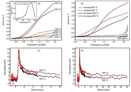
Fig.6 Sn-doped hematite and corresponding J-V charateristics80
3.2.2 Doping for narrowing electrode optical band gap
Besides enhanced conductivity that doping can lead to,it is also well recognized that doping with non-metal elements can induce band gap narrowing and thereby broaden the absorption spectrum of photoanode.In this respect,this strategy is to manipulate optical properties(ηLHE)rather than to adjust conductivity(ηtansport).Wide band gap of titanium dioxide and zinc oxide have impeded the possible efficient application for solar-assisted water cleavage.For instance,band gap width of 3.2 eV only renders the TiO2the possibility to achieve 1%limit of STH at most ideal condition8.To overcome the optical limitations of wide band gap semiconductors,carbon and nitrogen are used as dopants to narrow band gap of TiO2and ZnO50,58,81-84.Yang et al.85performed a density functional theory(DFT)calculation for electronic structure of both carbon-anion and carbon-cation-doped TiO2,predicting intra-band states induced by C could narrow optical band gap by up to 0.3 eV. The result indicated visible light absorption in TiO2could be allowed by those states,as evidenced by many experimental results83,86,87.In fact,experimental results were confirming that the effect of carbon doping come far before Yang′s prediction.Khan et al.81synthesized a chemically modified TiO2by natural gas combustion.The carbon species in combustion product were somehow doped into TiO2,which bestowed the dark metal oxides more pronounced performance in PEC water oxidation81.Furthermore,a carbon-doped TiO2nanotube fabricated by Bard and his coworkers83was first used in photoelectrochemical water splitting,which is able to respond to visible light(wavelength above 420 nm).
More recently,a facile nitrogen doping was reported by a lowtemperature annealing.As shown in Fig.7(a),the color of N2-treated BiVO4at 350°C turned darker compared to the pristine one.Most importantly,light absorption in spectral range above 500 nm,which is exactly the absorption edge of pristine BiVO4, was enhanced in line with the color change of N-doped samples (red line for N-doped sample,black for pristine one).To verify the valid conversion of incident photons to electrons,IPCE was measured as given in Fig.7(b),where the IPCE value in long wavelength range increased compared to pristine sample.That is, the incident photon with wavelength above 500 nm was not only taken in by N-doped BiVO4but also converted(though partially) to electrons that contributed to the Faradic current of the treated sample.This is also confirmed by the enhanced sulfate oxidation J-V characteristics in Fig.7(c).The surface kinetic barrier is excluded through the addition of vulnerable sulfate salt.Thereby, the elevated photocurrent(up to 5 mA·cm-2)under such consideration is deemed as larger hole/electron flux solely resulted in bulk factors(e.g.higher donor density and light harvesting efficiency),ruling out the kinetic effect induced by N2treating.According to experimental results,the extra charge caused by N substitution for O was compensated by creating excess amount of oxygen vacancies.DFT calculations with that consideration indicated a narrowed optical band gap(dropped by 0.3 eV)compared with pristine,as shown in Fig.7(d).The crystal structure of N-doped BiVO4is shown in Fig.7(e),with observation of an electron localized in vicinity of V atom.
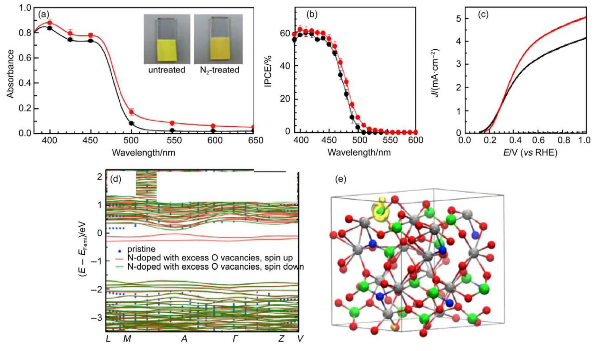
Fig.7 Effect of doping on light absorption by BiVO488
As the former example demonstrated,introducing nitrogen heteroatoms leaves more unbalanced negative charge in crystal structure.To neutralize those extra charges,oxygen vacancies are therefore created to compensate excessive electron added by N77,88. For substituting O2-with N3-
,two nitrogen atoms added will require three oxygen atoms leaving,equivalent to creating one oxygen vacancies.Those vacancies are known as the origin of ntype conductivity in many unintentionally doped metal oxide semiconductors.Besides heteroatom doping,annealing samples in a reducing atmosphere(e.g.H2)could introduce Ti3+,known as an equivalent entity for oxygen vacancies85,89,90.Li et al.91first demonstrated a reduced rutile nano-rods arrays on FTO substrates which generated high concentration of oxygen vacancies.The optical band gap is tuned in their case by the introduction of additional defect states,but visible light response of the photoanode was weak.The higher photocurrent fromH2-treated rutile(2.5 mA· cm-2at 1.23 V(vs RHE))was therefore attributed to higher donor density rather than light absorption,since those vacancies induced states are thermodynamically invalid for water cleavage.In this consideration,it could be concluded that color change of photoanode does not necessarily impart an effect on photocurrent. Nonetheless,hydrogen reduction has proved itself a reliable technique for enhancing PEC performance and we regraded it as a doping technique as well.For instance,Xie et al.5developed an Au-decorated TiO2photoanode with post-hydrogenation,delivering photocurrent around 3.0 mA·cm-2at 1.23 V(vs RHE). Hydrogenation brought about the formation of disorder layer atsurface attached with Au nanoparticles,as shown in Fig.8(a). Intriguingly,they found the sequence of the two treatment procedure,Au loading and hydrogenation,played a critical role in the photocurrent enhancement of TiO2.That is,the surface loaded Au facilitated the hydrogenation of photoanode,which was somehow related to the interaction of Au with hydrogen molecule activating H-H bond.As shown in Fig.8(b),when loaded withAu in advance of hydrogenation(H:Au/TiO2),the photocurrent of TiO2was much higher than that given by sample loaded with Au after hydrogen treating(Au/H:TiO2).Electron paramagnetic resonance(EPR) spectra in Fig.8(c)indicated more vacancies lied in H:Au/TiO2than Au/H:TiO2,possibly due to faster reduction rate as evidenced by temperature programmed reduction(TPR)spectra in H2atmosphere.The hydrogenation commenced at lower temperature forAu/TiO2in Fig.8(d).
3.2.3 Co-doping for synergistic effect or band tuning
Additional to single element doping,with two dopants one could expect their synergic effect in band structure adjustment76,77. As mentioned before,introduction of Ti3+or so-called oxygen vacancies in TiO2exceptionally increase donor density while enhanced light harvesting capability hardly contributed to photocurrent.Mullins et al.76discovered that the photoanode treated with both NH3and H2showed higher IPCE than those of either H2or NH3treated samples.They attributed the better performance from co-doping to the interactions between 3d state of Ti3+and N 2p state.The charge transfer resulted in more negative charged N atoms and higher energy level of N 2p.Recently,a case of codoping Mg and Zr into state-of-the-art Ta3N5photoanode proposed a band displacement effect with slightly band gap widening.As shown in Fig.9(a),Zr doping of Ta3N5shifted the photocurrent onset from 0.82 to 0.52 V(vs RHE),while Mg doping lifted photocurrent density maintaining original onset position.Incorporating the two dopants showed astonishing synergistic effect in both enhancing photocurrent density and advancing onset potential.Measurement of valence band maximum(VBM)and optical band gap were conducted,making it possible to estimate the position of conduction band minimum(CBM).The possible band structure is displayed in Fig.9(b).The shifts of both VBM and CBM to higher position by~0.2 eV were observed and attributed to co-doping technique.This higher position is in favor of water splitting at no expense of oxidative ability of the valence band holes,also the reason for advanced onset potential.
3.3 Building junctions
Similar to doping technique,building heterojunctions is exploited in semiconductor industries for photovoltaic devices to better collect photogenerated electron and hole in two opposite end of the device.Most of researchers tend to believe that the contact of two semiconductors with thermodynamically matched band structure will result in balancing of majority carrier in dark, leading to the spontaneous movement of carrier to or away fromthe contacting interface.The accumulation of charge at two ends of the interfacial contacting region was gradually saturated due to the opposite electric field generated by the accumulation itself.As a result,such contact caused the band bending at interface and relative change of band position could be observed92.The aims of building junctions are generally steered to following aspects:(a) increasing ηtransport,which is achieved readily when valid contact is established and optimized ratio of one semiconductor to the other are controlled93-96;(b)combining with enhanced light harvesting, namely combing a wide band-gap host to a narrow band-gap one97-99;(c)homojunction and gradient doping for consecutive potential drop and widened space charge layer45.
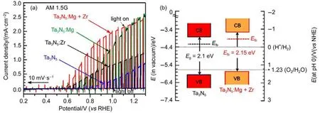
Fig.9 Co-doping and synergistic effect77
3.3.1 Heterojunctions for charge transport and separation
Deng et al.98developed a facile modification strategies for building heterojunction by exposing pristine FeOOH nano-rod arrays to TiCl4mist with controlled durations.After that,the sample was subjected to high temperature annealing up to 750°C to initiate the reaction between hematite and titanium-containing species.The result turned out to be that the photoanode is consisted of ultrathin Fe2TiO5coating layer covering Fe2O3nano-rods arrays and the J-V characteristics of hematite treated with different time are shown in Fig.10(a),where photocurrent density of the hybrid photoanode reached up to~1.5 mA·cm-2.IPCE,which reflected photon-to-electron conversion efficiency,indicated enhanced converted photon flux without a broadened light absorption spectrum(Fig.10(b)).That means the fabrication of Fe2O3/ Fe2TiO5hetero-junction did not affect the band gap energy, whereas the separation efficiency in bulk region could be elevated, according the proposed band alignment of the corresponding junction.In Fig.10(c),a typical n-n type band line-up shows the hole movement tendencies near their interface.The suitable match helped to form an n-n junction and facilitated the transferring of electrons from outer Fe2TiO5to inner Fe2O3,while holes from inner core to the surface coating.
p-n junction configuration with an n-type scaffold and p-type guest was also fabricated by Yuan et al.97.A polymer assisted fabrication procedures was used and the composited electrode exhibited astonishing photocurrent density up to 4.5 mA·cm-2at 1.23 V(vs RHE)in Fig.11(a).Due to the narrow band gap nature of Cu2O,the optical absorption range of the composited photoanode was largely broadened.Similarly,IPCE after Cu2O modification was augmented compared to pristine TiO2photoanode (Fig.11(b)).Therefore,a p-n junction aligning configuration was suggested by their estimations.In Fig.11(c),the two semiconductors after contact induce a bending of band position near their interface,due to the equilibrium of EFbetween n-type and p-type semiconductors.In this case,the photocurrent is largely elevated due to the introduction of Cu2O coating and hence better hydrogen production is verified,according to the authors.But some uncertainties in this conclusion lied in the fact that no measure of hydrogen production was conducted.It is also worth noting that Cu2O is vulnerable to oxidative condition and actual contribution of photocurrent in water splitting Faradic reaction are desired to be estimated from direct product detection.Moreover,the IPCE enhancement in visible region is weak compared to the large improvement in photocurrent.Without direct quantification of hydrogen production,it seems controversial that this modification facilitated charge transport for water cleavage since p-type materials possess a unfavorable downward band bending for hole transport to surface in contact with water,as shown in Fig.11(c). Despite the possible dispute this case might arouse,there are multiple cases which had verified the reliability of p-n junction building for enhanced water oxidation,including photoanodes like p-NiCo2O4/n-Si100,p-Co3O4/n-BiVO432,p-CaFe2O4/n-BiVO4101,p-MgFe2O4/n-Fe2O351and so on.
3.3.2 Heterojunctions combining with enhanced light harvesting
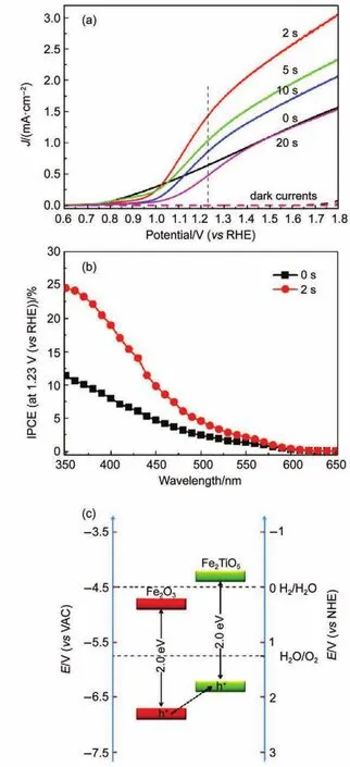
Fig.10 Fe2O3/Fe2TiO5N-N heterojunction98
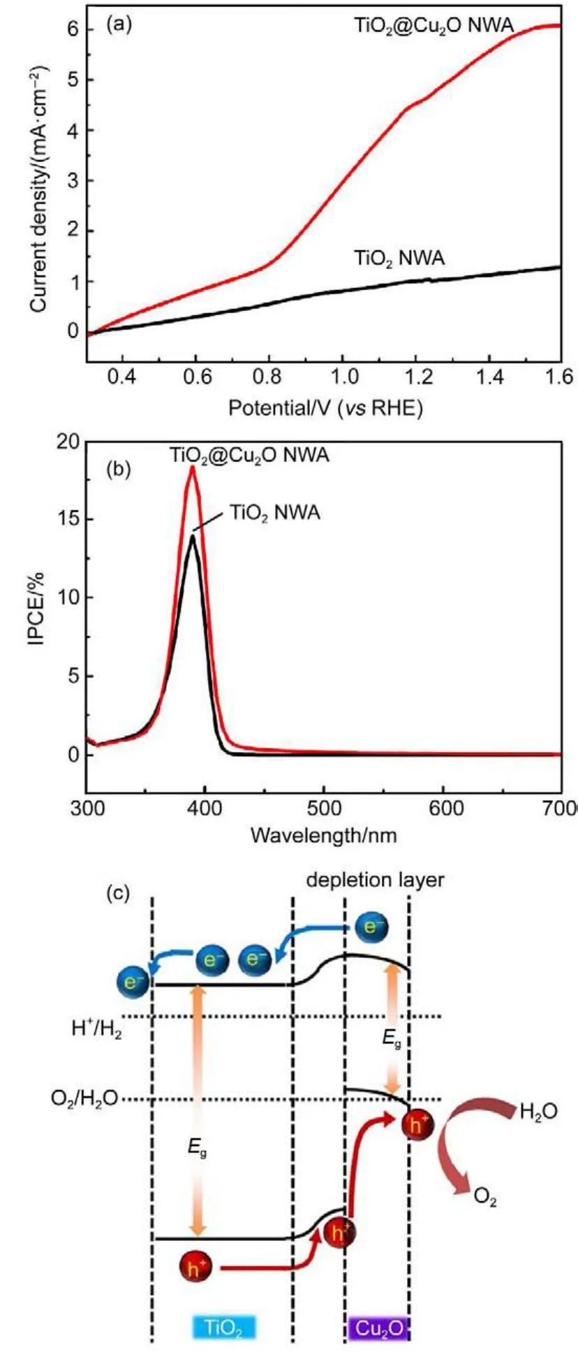
Fig.11 p-n heterojunction of TiO2/Cu2O97
In addition to internal electric field that helped to augment charge separation efficiency,light absorption could be adjusted by incorporating narrow band gap semiconductor with wide band gap scaffold32,44,61,99,102.In pursuit of that,a hole scaffold and guest absorber approach was proposed by Sivula et al.99Given the successful application of nanostructured TiO2scaffold with loaded dye molecules in dye-sensitized solar cells,they attempted to implement similar design with Fe2O3as light absorber and WO3as large-area support for electron collection.Near 20%increase in photocurrent was observed in WO3/Fe2O3host/guest photoanodes when compared with control sample.The improvement was also accompanied with the enhanced IPCE near absorption edge of Fe2O3in the hybrid electrode.This strategy proposed by Sivula et al.has been proved to be very effective in cases where the narrow band gap absorbers are well aligned with scaffold in thermodynamic considerations and it has been exploited to boost the photocurrent of wide band gap photoanode31,44,97,102,103.As a matter of fact,the resultant architectures not only make the best use of energy in solar spectrum,but also inherit virtues from the scaffolding nano-structure,which might weigh a lot in determination of the final photoelectrochemical performance.Therefore,further researches pertaining more complicated nanostructures loaded with visible light absorber are under extensive attention44,54.Liu et al.44reported a hybrid TiO2nano-tubes photoanode with ultra-thin Fe2TiO5coating for water splitting.The architecture of the photoanode is based on vertically aligned TiO2nanotubes array,which served as a nanostructured backbone,and a thin layer of Fe2TiO5decoration.As shown in Fig.12(a),the fabricated nanotubes arrays possesses porous structure with thin wall serving as shortcuts for hole transport to surface and facilitate the injection process as discussed in previous section.TEM images in Fig.12(b),reveals the interface between TiO2and Fe2TiO5.The low magnification image in the inset indicates the wall thickness is only around 10 nm where the Fe2TiO5is only about 2 nm thick.Theoretical cal-culation of band structure of TiO2and Fe2TiO5showed well matched band position,hence the contacting configuration shown in TEM observations will further promote the photogenerated hole to separate with electron,transport to the surface decorating Fe2TiO5,and finally inject into electrolyte.The measured IPCE in Fig.12(c)confirmed the largely improved photon conversion efficiency,where the absorption and“conversion”edge was shifted to over 700 nm.The APCE results considering absorbance in UV-Vis spectra were plotted in Fig.12(d).It is apparent to observe that the absorbed photons were effectively converted into excited electrons,further confirming the efficacy of nanostructured heterojunction with a higher ηtansport.As a result of incorporation with narrowband gap Fe2TiO5and a co-catalyst,the Fe2TiO5-TiO2/Cooxdelivered about 4.2 mA·cm-2of current density at 1.23 V(vs RHE)with maximal photoconversion efficiency of~2.7% (Fig.12(e)),far larger than pure TiO2can provide.
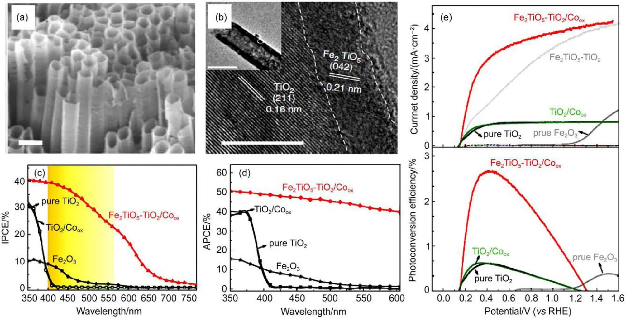
Fig.12 Heterojunction broadening absorption spectrum44
3.3.3 Homojunctions and gradient doping
For so many examples have discussed,it can now summarize that the essence of building junction is to construct an internal potential drop for electron moving from one material to another, which is realized by incorporating one semiconductor with another.In fact,such potential drop could be also introduced by a socalled gradient doping technique.This technique is classified as a junction building strategy because it involves the concept of homo-junction.As illustrated in Fig.13(a),W-doped and un-doped BiVO4photoanodes(W-BiVO4and BiVO4)possess the same band position while the EFof the two deviates from each other.For fabrication of a homo-junction,the two semiconductors are put into physical contact.Once in contact,the difference in EFis required to be balanced.Finally as an outcome of the thermal equilibrium,the band position of un-doped BiVO4moves upwards in relation to W-BiVO4and a drop of potential from W-BiVO4to the un-doped BiVO4is therefore developed.In light of this concept,an extension of homo-junction can be realized by gradually doping the photoanode from one to another depth interval with stepwise-increased dopant concentration,as shown in Fig.13(b). This was demonstrated by Abdi et al.45using spray pyrolysis with varied dopant concentration in different period of deposition.For gradient doping,the dopant concentration was changed stepwise every 20 deposition cycles(100 cycles in total),starting from 0% to 1%.Four samples were fabricated in the study:a homogeneously doped W-BiVO4photoanode,a homo-junction as shown in Fig.13(a)(W:BiVO4/BiVO4),a reverse homo-junction(BiVO4/ W:BiVO4)and a gradient doped BiVO4photoanode.In line with their expectations,gradient-doped BiVO4and homo-junction W: BiVO4/BiVO4did display better separation efficiency(ηtransport) compared to BiVO4/W:BiVO4and homogenously doped W-BiVO4(Fig.13(c)).J-V curves in Fig.13(d)manifests that this gradientdoped BiVO4delivered excellent photocurrent of 3.5 mA·cm-2at 1.23 V(vs RHE).Thickness of all the photoanodes were controlled to be the same,therefore it is reliable to surmise that the enhancement in photocurrent is originated from the development of gradient doped region.Thicker depletion region in gradient doped semiconductor was believed to be the reason for its better performance than homogeneously doped one.
3.4 Surface modification facilitating surface injection
There have been several strategies coping with issues lie in lightharvesting and charge transport,such as nanostructuring,doping and building junctions.These two processes,light absorption and charge transport,correspond to two measures of efficiency,ηLHEand ηtransport.Unsuitable Egand poor thickness control always limit ηLHEto be high at a broad spectral range,whereas recombination that happens in bulk region of the material greatly impedes ηtransportto be sufficient for practical use.However,besides the two processes take places in the bulk,charge injection into the electrolyte also played an important role in water oxidation,mainly to determine on-set potential and thus ηinjection.This process generally suffers from poor reaction kinetics and non-ideal surface structure, which deviate the practical photocurrent on-set cathodically(for photoanode)from flat band potential(EFB)of the semiconductor: on the one hand,poor surface injection kinetics for a redox reaction(oxygen evolution reaction in this case)required a large activation energy104,which is an obstacle rise from redox reaction itself;on the other hand,non-ideal surface structure(e.g.surface states which consume external biased voltage105,106)of a semiconductor might induce some unfavorable properties for charge transfer through electrode-electrolyte interface.
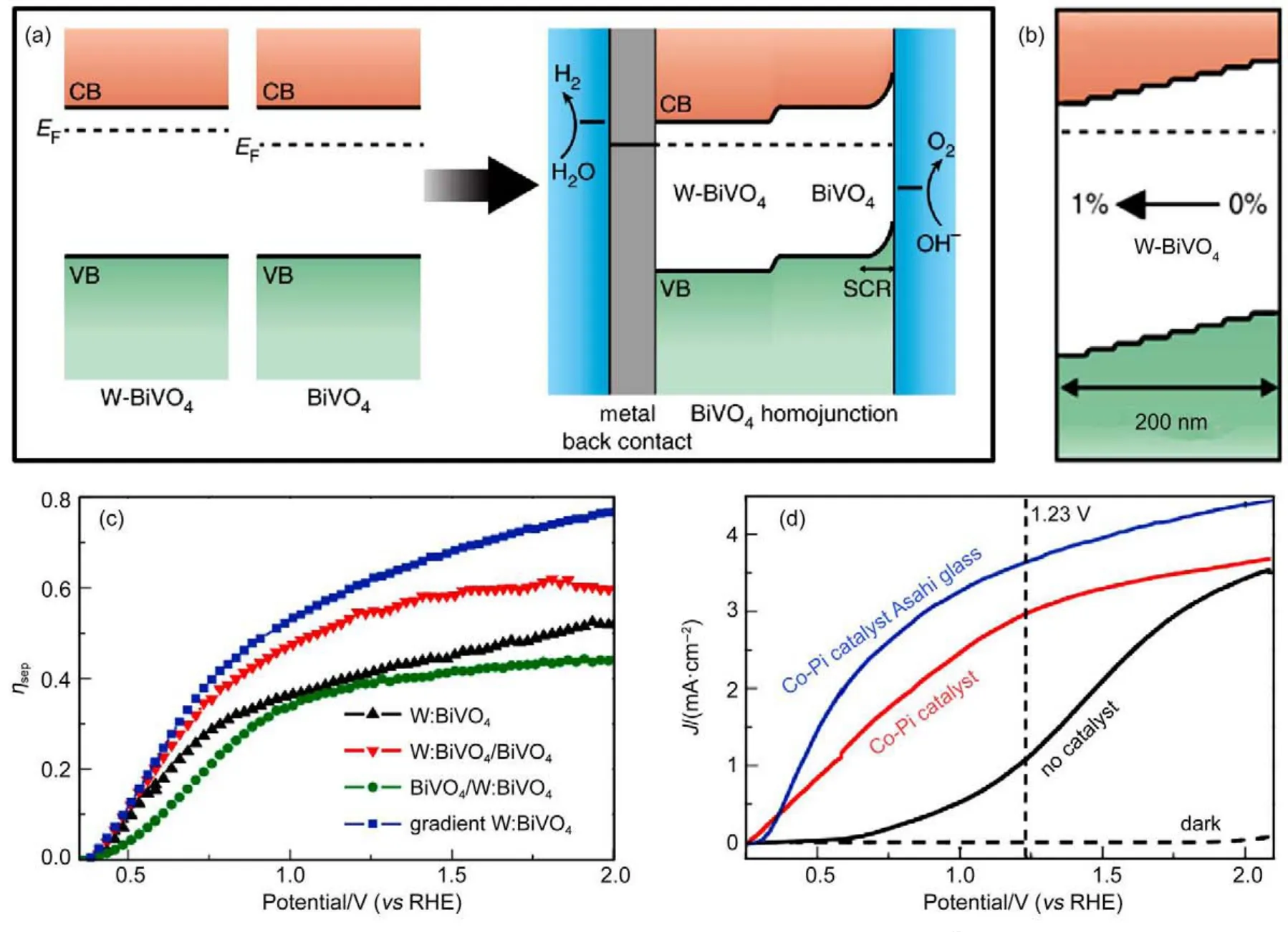
Fig.13 W:BiVO4/BiVO4homo-junction and gradient doping45
3.4.1 Utilization of catalyst for improved injection
In order to illustrate the effect of surface coated catalyst on photoanode,Tilley et al.107proposed an ideal J-V curve for hematite electrode.The maximal photocurrent of non-ideal hematite photoanode is limited to only several mili-amperes per square centimeter,due to the charge recombination in bulk and poor surface kinetics.For an ideal hematite photoanode,the maximal photocurrent should be up to~12 mA·cm-2based on its Eg,while on-set potential at 0.4 V(vs RHE)according to its EFB.To realize that,strategies such as nanostructuring as we have discussed could be implemented to overcome the recombination issue in bulk and to restore to the ideal photocurrent,while catalyst loading could be used for reducing over-potential in order to advance on-set potential back to the ideal EFB.
Generally speaking,co-catalysts that have been implemented for photoanode to dates are quite complicated.Catalysts such as Co-Pi29,108,109,Co-Ci110,Ni-Bi111,and hydroxides like FeOOH27,55had been widely applied as catalyst to lower reaction barriers.Due to the fact that these catalyst are commonly porous,hydrated,redoxactive,nanostructured or non-crystalline,it is extremely hard to describe such material and accordingly to analyze them112.And also,based on the complexity of such subject,many practical factors might prevent the catalyst layer to function well as expected.One of the most attractive cases pertaining catalyst loading was demonstrated by Kim and Choi27.In their study,a nano-porous BiVO4photoanode was modified by dual layer OER catalyst, namely FeOOH and NiOOH in different sequences to achieve advanced on-set potential and higher ηinjection.Optimized photocurrent of 2.73 mA·cm-2at 0.6 V(vs RHE)could be obtained using the resulting BiVO4/FeOOH/NiOOH photoanode.Inter-estingly,they turned out to discover that surface modified photoanodes manifest different photocurrent densities,depending on the types and sequence of catalysts loaded.Only when FeOOH was coated at first followed by NiOOH deposition can the BiVO4reach an optimized photocurrent response.In order to gain insight into enhancement of ηinjection,Na2SO3was added into electrolyte to erase reaction barrier.According to the principal for ηinjectioncalculations,the efficiency was obtained by dividing Jphfor water oxidation with Jscavfor sulfite oxidation.Based on this,they observed that BiVO4/FeOOH/NiOOH also possesses the best injection efficiency,better than BiVO4/NiOOH/FeOOH with reverse catalyst sequence.Mott-Schottky measurement of all the photoanodes had demonstrated same donor density while the shifts in EFBwere observed after loading catalyst.This had led the authors to attribute the deviation of EFBto the change in zero-point potential induced by the outmost layer of catalyst,since it is the only other factor might change EFB.According to the experimental facts of this example,OER catalyst dose exert a great influence in photocurrent onset and the extent of improvement could be further optimized by the manner of catalyst incorporation.Choi′s case had used photo-assisted deposition method to incorporate OER electrocatalyst with semiconductor.Actually,even the experiment method researchers used for loading catalyst might influence the final effect on the extent of onset potential shift and photocurrent increase.For instance,Zhong et al.109discovered performance of hematite photoanodes largely differ from one another based on the loading manner and state of Co-Pi on hematite.As shown in Fig.14 (a-c),the mechanism of catalyst deposition by photo-assisted electrodeposition,pure electrodeposition and wet impregnation are illustrated.The morphologies resulted from three different deposition strategies are almost the same,according to SEM images (Fig.14(d-f)).However,catalysts loaded through the three methods showed absolutely different ability to advance onset potential and increase photocurrent.As plotted in column charts in Fig.14(g),photo-assisted electrodeposition induced a large cathodic shift up to 170 mV in photocurrent onset,compared with ~100 mV for electrodeposition and~80 mV for wet impregnation technique.Similarly,increase in photocurrent resulting fromphotoassisted electrodeposition is the most obvious as well,which is up to~1.4 mA·cm-2.
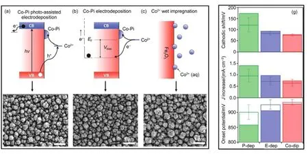
Fig.14 Effect of deposition manner as a co-catalyst with photoanode109
The example using photo-assisted electrodeposition method showed that somehow the loading method influenced the performance of OER catalyst at photoanode surface.Variations in the extent photocurrent and on-set potential improvement was attributed to the more selective loading site that photo-assisted deposition induced.It is worth noting that the photo-assisted electrodeposition method only applies a small voltage between working electrode and counter electrode,which is only sufficient to deposit catalyst under illumination.Therefore,only positions with“stronger”oxidation ability would selectively oxidize catalyst species(Co2+in this case)and this might be the reason for better performance given by photo-assisted deposition method. Following research given by Li et al.48directly observed a spatial separation in hole and electron transfer direction when using photo-deposition method to incorporate co-catalyst onto BiVO4with well-defined crystal facets exposed at surface.As shown in Fig.15(a-c),it was discovered that metal like silver and platinum are more likely to be deposited at{010}facets while metal oxides like PbO2and MnOxare more likely to be deposited at{110} facets.Because the metal ions are reduced to metal,it can beaccordingly to assume that photo-reduction are more inclined to happen at{010}facets,which means that electrons are more concentrated at those facets.{110}facets that facilitate photooxidation are hence defined as hole-concentrated regions.This naturally gives us a vision that when HER catalyst could be selectively loaded at{010}facets and OER catalysts at{110}facets, optimized performance could be achieved.Indeed,the oxygen evolution amount of BiVO4with both photo-deposited Pt and MnOxoutnumber other samples in pure photocatalytic water oxidation experiment.In PEC water splitting(Fig.15(d)),BiVO4with photo-deposited MnOxpossessed the best photocurrent output.This case,along with previous one pertaining photo-assisted deposition,unraveled the importance of this“site selectivity”of HER or OER catalyst at photocatalyst surface.

Fig.15 Spatial separation of carriers at BiVO4single crystal and its influence on photocurrent48
Cobalt and nickel based metal oxides,such as Co3O4,NiO and NiCo2O4,are known as well-performed catalyst for oxygen evolution as well as p-type semiconductor32,100,113-116.Once they were put into connection with n-type photoanode,a p-n junction with superior surface catalytic performance will be formed.In an example given by Chang et al.32,suspension of a p-type electrocatalytic active Co3O4was dropped on n-type BiVO4photoanode followed by annealing treatment to enhance physical contact.This allowed the formation of p-n junction where bands of Co3O4shifted upward due to thermal equilibrium as shown in Fig.16(a), creating potential drop whereas maintaining sufficiently positive valence band position for oxygen evolution.Resultant photoanode delivered an optimized current density more of 2.5 mA·cm-2at 1.23 V(vs RHE).It was henceforth attributed better bulk separation and faster surface injection.Calculation of ηbulk(ηtransport)was demonstrated in Fig.16(b)as a function of potential to verify contribution from facilitated separation.As discussed in a previous section,ηtransportcomes from the ratio of Jscavto Jabsand reflects the efficiency of charge separation and transport.Therefore,the lifted ηtransportshown in the figure corresponds to a better separation as a result of p-n junction formation.Besides,it was also observed that Co3O4with favorable surface properties brought a forward shift in current onset for pure electro-catalytic water splitting in dark, while this difference was eliminated by the addition of hole scavenger(Fig.16(c,d)).Such behavior discovers the catalytic ability for OER while the elimination of difference achieved by scavenger indicates the reliability of the aforementioned assumption in ηinjectioncalculation:reaction barrier could be erased by scavenger,giving 100%of ηinjection.The calculation of ηinjection,in this cased termed as ηsurface,was displayed in Fig.16(e),where thehighest injection efficiency was reached by the optimized Co3O4/ BiVO4composite.In summary,this work first separately unearthed the bulk and surface contribution by building a heterojunction,showing a promising strategy that succedent researchers can look into.

Fig.16 Simultaneous enhancement in photocurrent and onset32
Although there are many cases successfully realizing advanced photoanode onset with catalyst,mechanism of catalysts on photoanode are not well analyzed,especially for those without welldefined structure(e.g.Co-Pi).Nonetheless,many have managed to probe the reaction kinetics and energetics for the cathodic shift and photocurrent enhancement induced by OER co-catalyst.Some claimed that the photo-generated hole in photoanode is instantly trapped in excelling water-oxidation catalyst layer and then transfer to water with faster kinetics,which also enhanced electron gradient in the bulk of the host material117.Some also contended that reaction barrier is reduced by coupling hole induced oxidation reaction of multivalent species and water oxidation process(e.g. from Co2+to Co3+and Co4+,which is then reduced by water)49,118. Others suggested a junction formation increasing band bending and negatively shifting EFB119.Due to the complexity of this system,Nellist et al.112attempted to classify those catalyst into two classification:“volume”catalyst and“surface”catalyst.The former is ion-permeable allowing catalysis throughout its volume, while the latter only restricts the catalytic behavior at surface.In this context,sparse catalysts(loose and ion-permeable)like NiOOH,FeOOH,Co-Pi,and Ni-Bi,are categorized as volume catalyst forming adaptive junction,whereas dense catalysts like Pt,IrO2,and Co3O4,are regarded as surface ones forming buried junction.Accordingly,they developed a double working-electrode PEC technique where the potential of semiconductor and potential at catalyst surface were managed to be measured.Experiment results had proved that potential drop through semiconductor and catalyst interface varied with adjusted applied potential on semiconductor,which could not be accounted for by traditional semiconductor junction model or equivalent-circuit model.Based on investigation results,this research concluded on a new model for catalyst loading on a semiconductor electrode,meanwhile showing that the complexity and difficulties lie in the study of semiconductor-catalyst interfaces.
3.4.2 Surface states and their passivation
As for passivation layer,it was more frequently implemented in hematite photoanodes,which in fact is a layer of relatively insulating ultra-thin metal oxide or semiconductor coating with wide band gap.In the interpretation of passivation effect,some contended that the passivation effect is not a true catalytic effect, but rather an elimination of unfavorable surface termination of semiconductor120.Thereby,surface states(STs)are normally regarded as the energetic counterpart for such unfavorable surface termination in band diagrams,which are introduced to explain their effects in charge transfer through semiconductor-electrolyte interface.For n-type semiconductor,these originally occupied and localized electronic states usually situate in band gap.For hematite again,Klahr et al.105once discovered a ST capacitance charging effect in the photoanode and measured the energy levels of these surface states using electrochemical impedance spectrum analysis. Results ended up suggesting that these states are located at just slightly positive than water oxidation potential(1.23 V(vs RHE)) but more negative than valence band,as shown at Fig.17(a)with two measures in neutral and basic conditions.In that context,holes that generated in hematite should be more inclined to first transferto those states then to water.The traditional band diagram and possible carrier transfer pathway are illustrated in Fig.17(b).STs here are represented by trap states lie between semiconductor and electrolyte.Once the Fermi level are tuned by applied bias to a more positive position than that of STs,these pre-occupied states will be first emptied by holes from photoanode,leaving positive charges at surface.The presence of surface positive charges attenuates the potential drop across surface,reduce band bending and accordingly shift EFBpositively,which generally explains why the passivation of STs advances photocurrent onset7.
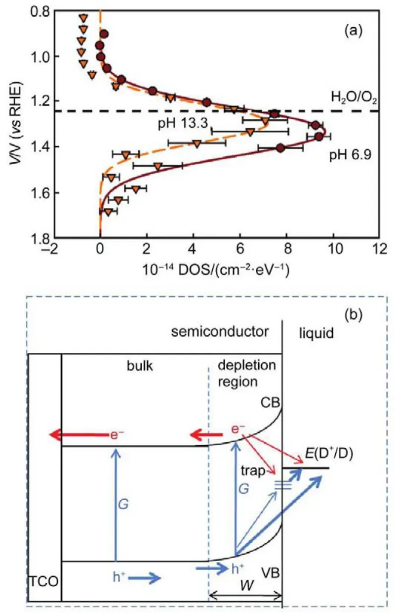
Fig.17 Measurement of STs and charge transfer during ST present105

Fig.18 Hematite electrode passivated by thin metal oxide layer106
The chemical origin for the generation of STs is assumed to be surface hydroxyl group,dangling oxygen or other surface impurities7,110,121.Therefore,passivating STs is to either shield those surface termination from contact with water or just simply eliminate them to facilitate direct VB to electrolyte injection.To be more specific,strategies to passivate STs commonly involve ultra-thin layer coating,accomplished by techniques like atomic layer deposition(ALD)106,116.This technique was able to cover electrode surface with ultra-thin metal oxide layer such as Al2O3, Ga2O3and TiO2,and thus shielding photoanode from direct contact with electrolyte and changing surface environment106,120,122,123.Due to the fact that EFBof a ST-rich photoanode is dependent on the corresponding ST density,erase of ST effect will naturally lead to the negative shift of EFB124.Accordingly,if the surface termination is rectified,photocurrent should be advanced to a more cathodic position(for photoanode),similar to the result of OER catalyst loading.As shown in Fig.18(a)demonstrated by Le Formal et al.106,the photocurrent transient spikes measured at chopped light condition was flattened upon Al2O3deposition.This had been interpreted as reduced hole accumulation at surface resulting from faster hole injection.Also as shown in Fig.18(b),the effect ofALD deposited Al2O3is actually mild in lifting photocurrent density but obvious in changing the onset point of current to a lower potential. Acathodic shift of more than 100 mV in onset potential could be achieved by only Al2O3deposition.Furthermore,on the basis of coating Al2O3more advanced current onset was obtained by Co2+absorption treatment.The Co2+absorption here was distinguished from surface passivation and its effect was regarded as purely electro-catalytic.However,since catalytic effect can quicken hole transfer thus to promote current onset as well as to reduce surface hole accumulation,attention are necessary to be paid to rule out the possibility of catalytic effect fromAl2O3.Thereby,similar Al3+absorption and post-annealing treatment was applied to hematite, which resulted in no improvement of onset potential.Experiment findings substantially confirmed that the passivation effect induced by Al2O3coating is another aspect for improving surface injection.Also,the authors also claimed that surface passivation technique,if combined with electrocatalyst,could help to moveforward to a more excelling photoanode operating at low potential. It was proven by a subsequent study by Steier et al.116combining Nb2O5with co-catalyst,where the metal oxide layer shifted the energetic distribution to a more negative potential region enabling faster STs charging and more negative onset.
4 Conclusions and outlooks
In general,this review is aimed to help reader to have a fast glance on various effective strategies for improving some important metrics of PEC system,mainly focusing on photoanode cases.Brief introduction on operating principals and several important parameters and types of PEC system have been included into the paper as a broader context.Despite that,the main theme of this review is on efficient and reliable modification strategies for elevating practical performance.These strategies,based on their operating features,are categorized into four classifications, including nanostructuring,doping,junction building and surface injection modification.Also,in each section,attempts are made to further split those four general types of strategies into sub-types according to how the strategies function and what effect they impart on photoanode properties.Complete photolysis process generally consisted of(a)light absorption,(b)charge transfer,(c) redox reaction or carrier injection,(d)adsorption,desorption,and mass diffusion of chemical species,and(e)charge recombination. These steps are more or less influenced by the applied strategies, therefore leading to the final improvement.Under this consideration,the exact affected metrics are pointed out during the elaboration on modification strategies.For instance,amongst those major photolysis steps light absorption could be influenced by light scattering from nanostructure,doping-tuned band gap, hetero-junction with visible light absorber.Accordingly,metrics concerning light absorption,such as ηLHE,IPCE,and APCE,could be perturbed by optical property variations and such changes have been intentionally discussed.
In fact,the whole picture of all the strategies has unanimously showed a general aim to produce oxygen evolution photocurrent as high as possible at a considerably low applied bias.This feature is critical for whether the photoanode is able to be incorporated into tandem cell powered by photovoltaic device without external bias110,125,126To reach out for better practical output closing up to the idealized calculations,one should elevate the maximal photocurrent plateaus and meanwhile reduce reaction over-potential for early onset.By implementing nanostructure,doping,heterojunction,optimized photocurrent could be achieved,while loading catalysis and surface engineer have partially resolved kinetics issues and advanced current onset to one benchmark to another107,116.Still,the photocurrent bottleneck nowadays keeps preventing PEC water splitting from scalable practice.In this perspective and in light of the existing strategies,we put forward as follows several points that might be instructive for fabricating photoanode in future demand.
(1)Light harvesting capability are still desirable to be multiplied from two perspectives:increasing the portion of valid light absorption and searching for materials with better gap valence and conduction band.In addition,the possibility of implementing more light-relating physical effects should be investigated.For instance,light-induced surface plasmon resonance effect has been adopted in enhancing PEC performance,while its detailed mechanism in water splitting is still not well resolved127-131. Moreover,carbon quantum dots were found somehow beneficial for PEC system,whereas deep discussions on how they promoted photoresponse are lacked132.These examples are different from traditional consideration for building composited photoelectrode. Therefore,understanding of these new methods and the possible different physical effect lying behind phenomena are imperative to be gained.
(2)Nanostructuring is realized to be useful in facilitating diffusion,while heterojunction building with visible light absorber drastically augments light harvesting.The combination of the two techniques have been long proposed99,and have been proved to be very effective up to dates,serving as an excellent precedent uncovering that combining the merits from each of these strategies could yield more powerful photoelectrodes for PEC hydrogen generation.Thereby,preceding to a more complex design with several modification strategies together might be a promising aspect as to develop high-performance photoanode.
(3)Catalyst and the somehow vaguely defined surface states passivation techniques have improved a lot in photocurrent onset and also manifested multiple difficulties to further study on their detailed behaviors at a smaller scope.As a matter of fact,even the semiconductor-catalyst interface was deemed to be extremely complicated47,48,133-135.The study for obtaining insight in this perspective remains nearly as a virgin land to be explored and shall provide numerous useful conclusions help to fully comprehend on why the photocurrent onset deviates far from EFBand how to eliminate those unfavorable factors delaying OER onset on photoanode.
(4)Despite numerous reports about all these effective strategies, in some situations nanostructuring,doping,junction building or surface passivation are not that effective or they might only appear to be effective.Since the major indicator we adopted to evaluate the effectiveness of these approaches in laboratory basically is the enhancement in current density.Other aspects(stability,byproducts,performance in full PEC configuration and so on)influencing their actual application prospect are fundamentally more vital.For instance,the stability of the photoanode is critical for low-cost,scalable and sustainable application in future.Are these strategies all so effective in long term testing(up to hours)?And how does the deterioration of photocurrent happen,the mechanism of losing performance and its prevention?They could be the more urgent aspects remained to explore.
(1)Hisatomi,T.;Kubota,J.;Domen,K.Chem.Soc.Rev.2014,43, 7520.doi:10.1039/c3cs60378d
(2)Fujishima,A.;Honda,K.Nature 1972,238,37.doi:10.1038/238037a0
(3)Gan,J.;Lu,X.;Tong,Y.Nanoscale 2014,6,7142. doi:10.1039/c4nr01181c
(4)Lu,X.;Xie,S.;Yang,H.;Tong,Y.;Ji,H.Chem.Soc.Rev. 2014,43,7581.doi:10.1039/c3cs60392j
(5)Xie,S.;Li,M.;Wei,W.;Zhai,T.;Fang,P.;Qiu,R.;Lu,X.; Tong,Y.Nano Energy 2014,10,313.doi:10.1016/j. nanoen.2014.09.029
(6)Yang,Y.;Ling,Y.;Wang,G.;Liu,T.;Wang,F.;Zhai,T.;Tong, Y.;Li,Y.Nano Lett.2015,15,7051.doi:10.1021/acs. nanolett.5b03114
(7)Li,T.;He,J.;Peña,B.;Berlinguette,C.P.Angew.Chem.Int. Edit.2016,55,1769.doi:10.1002/anie.201509567
(8)Chen,Z.;Dinh,H.N.;Miller,E.Photoelectrochemical Water Splitting;Springer:Heidelberg,2013;pp 1-15.
(9)Miller,E.L.Energy Environ.Sci.2015,8,2809.doi:10.1039/ C5EE90047F
(10)Li,R.;Weng,Y.;Zhou,X.;Wang,X.;Mi,Y.;Chong,R.;Han, H.;Li,C.Energy Environ.Sci.2015,8,2377.doi:10.1039/ c5ee01398d
(11)Wolcott,A.;Smith,W.A.;Kuykendall,T.R.;Zhao,Y.;Zhang, J.Z.Small 2009,5,104.doi:10.1002/smll.200800902
(12)Wang,H.;Deutsch,T.;Turner,J.A.J.Electrochem.Soc. 2008,155,F91.doi:10.1149/1.2888477
(13)Feng,K.;Li,W.;Xie,S.;Lu,X.Electrochim.Acta 2014,137, 108.doi:10.1016/j.electacta.2014.05.152
(14)Cesar,I.;Kay,A.;Gonzalez Martinez,J.A.;Grätzel,M.J.Am. Chem.Soc.2006,128,4582.doi:10.1021/ja060292p
(15)Rahman,M.A.;Bazargan,S.;Srivastava,S.;Wang,X.;Abd-Ellah,M.;Thomas,J.P.;Heinig,N.F.;Pradhan,D.;Leung,K. T.Energy Environ.Sci.2015,8,3363.doi:10.1039/ c5ee01615k
(16)Hu,Y.S.;Kleiman-Shwarsctein,A.;Forman,A.J.;Hazen,D.; Park,J.N.;McFarland,E.W.Chem.Mater.2008,20,3803. doi:10.1021/cm800144q
(17)Cho,S.K.;Park,H.S.;Lee,H.C.;Nam,K.M.;Bard,A.J. J.Phys.Chem.C 2013,117,23048.doi:10.1021/jp408619u
(18)Chen,L.;Toma,F.M.;Cooper,J.K.;Lyon,A.;Lin,Y.;Sharp, I.D.;Ager,J.W.ChemSusChem 2015,8,1066.doi:10.1002/ cssc.201402984
(19)Tong,L.;Iwase,A.;Nattestad,A.;Bach,Udo.;Weidelener,M.; Gotz,G.;Mishra,A.;Bauerle,P.;Amal,R.;Wallace,G.G.; Mozer,A.J.Energy Environ.Sci.2012,5,9472.doi:10.1039/ C2EE22866A
(20)Su,J.;Guo,L.;Bao,N.;Grimes,C.A.Nano Lett.2011,11, 1928.doi:10.1021/nl2000743
(21)Rao,P.M.;Cai,L.;Liu,C.;Cho,I.S.;Lee,C.H.;Weisse,J. M.;Yang,P.;Zheng,X.Nano Lett.2014,14,1099. doi:10.1021/nl500022z
(22)Higashi,M.;Domen,K.;Abe,R.J.Am.Chem.Soc.2012,134, 6968.doi:10.1021/ja302059g
(23)Ding,C.;Shi,J.;Wang,D.;Wang,Z.;Wang,N.;Liu,G.; Xiong,F.;Li,C.Phys.Chem.Chem.Phys.2013,15,4589. doi:10.1039/c3cp50295c
(24)Abdi,F.F.;van de Krol,R.J.Phys.Chem.C 2012,116,9398. doi:10.1021/jp3007552
(25)Abdi,F.F.;Firet,N.;van de Krol,R.ChemCatChem 2013,5, 490.doi:10.1002/cctc.201200472.
(26)Walter,M.G.;Warren,E.L.;McKone,J.R.;Boettcher,S.W.; Mi,Q.;Santori,E.A.;Lewis,N.S.Chem.Rev.2010,110, 6446.doi:10.1021/cr1002326
(27)Kim,T.W.;Choi,K.S.Science 2014,343,990.doi:10.1126/ science.1246913
(28)Qiu,W.;Huang,Y.;Long,B.;Li,H.;Tong,Y.;Ji,H. Chem.-Eur.J.2015,21,19250.doi:10.1002/chem.201503261
(29)Zhong,D.K.;Choi,S.;Gamelin,D.R.J.Am.Chem.Soc. 2011,133,18370.doi:10.1021/ja207348x
(30)Dotan,H.;Sivula,K.;Grätzel,M.;Rothschild,A.;Warren,S. C.Energy Environ.Sci.2011,4,958.doi:10.1039/c0ee00570c
(31)Shi,X.;Choi,I.Y.;Zhang,K.;Kwon,J.;Kim,D.Y.;Lee,J. K.;Oh,S.H.;Kim,J.K.;Park,J.H.Nat.Comm.2014,5, 4775.doi:10.1038/ncomms5775
(32)Chang,X.;Wang,T.;Zhang,P.;Zhang,J.;Li,A.;Gong,J. J.Am.Chem.Soc.2015,137,8356.doi:10.1021/jacs.5b04186
(33)Rettie,A.J.;Lee,H.C.;Marshall,L.G.;Lin,J.F.;Capan,C.; Lindemuth,J.;McCloy,J.S.;Zhou,J.;Bard,A.J.;Mullins,C. B.J.Am.Chem.Soc.2013,135,11389.doi:10.1021/ ja405550k
(34)Hahn,N.T.;Ye,H.;Flaherty,D.W.;Bard,A.J.;Mullins,C.B. ACS Nano 2010,4,1977.doi:10.1021/nn100032y
(35)Pihosh,Y.;Turkevych,I.;Mawatari,K.;Uemura,J.;Kazoe,Y.; Kosar,S.;Makita,K.;Sugaya,T.;Matsui,T.;Fujita,D.;Tosa, M.;Kondo,M.;Kitamori,T.Sci.Rep.2015,5,11141. doi:10.1038/srep11141
(36)Li,M.;Zhang,Z.;Lyu,F.;He,X.;Liang,Z.;Balogun,M.S.; Lu,X.;Fang,P.P.;Tong,Y.Electrochim.Acta 2015,186,95. doi:10.1016/j.electacta.2015.10.048
(37)Peng,Q.;Kalanyan,B.;Hoertz,P.G.;Miller,A.;Kim,D.H.; Hanson,K.;Alibabaei,L.;Liu,J.;Meyer,T.J.;Parsons,G.N.; Glass,J.T.Nano Lett.2013,13,1481.doi:10.1021/nl3045525
(38)Mohapatra,S.K.;John,S.E.;Banerjee,S.;Misra,M.Chem. Mater.2009,21,3048.doi:10.1021/cm8030208
(39)Xu,M.;Da,P.;Wu,H.;Zhao,D.;Zheng,G.Nano Lett.2012, 12,1503.doi:10.1021/nl2042968
(40)Wang,G.;Ling,Y.;Wheeler,D.A.;George,K.E.;Horsley, K.;Heske,C.;Zhang,J.Z.;Li,Y.Nano Lett.2011,11,3503. doi:10.1021/nl202316j
(41)Kleiman-Shwarsctein,A.;Hu,Y.S.;Forman,A.J.;Stucky,G. D.;McFarland,E.W.J.Phys.Chem.C 2008,112,15900. doi:10.1021/jp803775j
(42)Zhang,P.;Kleiman-Shwarsctein,A.;Hu,Y.S.;Lefton,J.; Sharma,S.;Forman,A.J.;McFarland,E.Energy Environ.Sci.2011,4,1020.doi:10.1039/c0ee00656d
(43)Pilli,S.K.;Deutsch,T.G.;Furtak,T.E.;Brown,L.D.;Turner, J.A.;Herring,A.M.Phys.Chem.Chem.Phys.2013,15,3273. doi:10.1039/c2cp44577H
(44)Liu,Q.;He,J.;Yao,T.;Sun,Z.;Cheng,W.;He,S.;Xie,Y.; Peng,Y.;Cheng,H.;Sun,Y.;Jiang,Y.;Hu,F.;Xie,Z.;Yan, W.;Pan,Z.;Wu,Z.;Wei,S.Nat.Commun.2014,5,5122. doi:10.1038/ncomms6122
(45)Abdi,F.F.;Han,L.;Smets,A.H.;Zeman,M.;Dam,B.;van de Krol,R.Nat.Commun.2013,4,2195.doi:10.1038/ ncomms3195
(46)Coridan,R.H.;Arpin,K.A.;Brunschwig,B.S.;Braun,P.V.; Lewis,N.S.Nano Lett.2014,14,2310.doi:10.1021/nl404623t
(47)Lin,F.;Boettcher,S.W.Nat.Mater.2014,13,81. doi:10.1038/nmat3811
(48)Li,R.;Zhang,F.;Wang,D.;Yang,J.;Li,M.;Zhu,J.;Zhou,X.; Han,H.;Li,C.Nat.Commun.2013,4,1432.doi:10.1038/ ncomms2401
(49)Wang,G.;Ling,Y.;Lu,X.;Zhai,T.;Qian,F.;Tong,Y.;Li,Y. Nanoscale 2013,5,4129.doi:10.1039/c3nr00569k
(50)Xie,S.;Lu,X.;Zhai,T.;Li,W.;Yu,M.;Liang,C.;Tong,Y. J.Mater.Chem.2012,22,14272.doi:10.1039/c2jm32605a
(51)Hou,Y.;Zuo,F.;Dagg,A.;Feng,P.Angew.Chem.2013,125, 1286.doi:10.1002/ange.201207578
(52)Li,M.;Zhang,Z.;Lyu,F.;He,X.;Liang,Z.;Balogun,M.;Lu, X.;Fang,P.;Tong,Y.Electrochim.Acta 2015,186,95. doi:00.1016/j.electacta.2015.10.048
(53)Su,J.;Feng,X.;Sloppy,J.D.;Guo,L.;Grimes,C.A.Nano Lett.2011,11,203.doi:10.1021/nl1034573
(54)Hou,Y.;Zuo,F.;Dagg,A.P.;Liu,J.;Feng,P.Adv.Mater. 2014,26,5043.doi:10.1002/adma.201401032
(55)Yu,Q.;Meng,X.;Wang,T.;Li,P.;Ye,J.Adv.Funct.Mater. 2015,25,2686.doi:10.1002/adfm.201500383
(56)Li,W.;Da,P.;Zhang,Y.;Wang,Y.;Lin,X.;Gong,X.;Zheng, G.ACS Nano 2014,8,11770.doi:10.1021/nn5053684
(57)Mohapatra,S.K.;Misra,M.;Mahajan,V.K.;Raja,K.S. J.Phys.Chem.C 2007,111,8677.doi:10.1021/jp071906v
(58)Kim,H.I.;Monllor-Satoca,D.;Kim,W.;Choi,W.Energy Environ.Sci.2015,8,247.doi:10.1039/c4ee02169J
(59)Zhang,Z.;Zhang,L.;Hedhili,M.N.;Zhang,H.;Wang,P. Nano Lett.2013,13,14.doi:10.1021/nl3029202
(60)Grigorescu,S.;Bärhausen,B.;Wang,L.;Mazare,A.;Yoo,J. E.;Hahn,R.;Schmuki,P.Electrochem.Commun.2015,51,85. doi:10.1016/j.elecom.2014.12.019
(61)Reyes-Gil,K.R.;Robinson,D.B.ACS Appl.Mater.Inter. 2013,5,12400.doi:10.1021/am403369p
(62)McDonald,K.J.;Choi,K.S.Energy Environ.Sci.2012,5, 8553.doi:10.1039/c2ee22608a
(63)Jia,Q.;Lwashina,K.;Kudo,A.Proc.Natl.Acad.Sci.U.S.A. 2012,109,11564.doi:10.1073/pnas.1204623109
(64)Hodes,G.;Cahen,D.;Manassen,J.Nature 1976,260,312. doi:10.1038/260312a0
(65)Li,L.;Yu,Y.;Meng,F.;Tan,Y.;Hamers,R.J.;Jin,S.Nano Lett.2012,12,724.doi:10.1021/nl2036854
(66)Vayssieres,L.;Sathe,C.;Butorin,S.M.;Shuh,D.K.; Nordgren,J.;Guo,J.Adv.Mater.2005,17,2320.doi:10.1002/ adma.200500992
(67)Mor,G.K.;Shankar,K.;Paulose,M.;Varghese,O.K.; Grimes,C.A.Nano Lett.2005,5,191.doi:10.1021/nl048301k
(68)Cho,I.S.;Chen,Z.;Forman,A.J.;Kim,D.R.;Rao,P.M.; Jaramillo,T.F.;Zheng,X.Nano Lett.2011,11,4978. doi:10.1021/nl2029392
(69)Liang,S.;He,J.;Sun,Z.;Liu,Q.;Jiang,Y.;Cheng,H.;He,B.; Xie,Z.;Wei,S.J.Phys.Chem.C 2012,116,9049. doi:10.1021/jp300552s
(70)Cesar,I.;Sivula,K.;Kay,A.;Zboril,R.;Grätzel,M.J.Phys. Chem.C 2008,113,772.doi:10.1021/jp809060p
(71)Zhou,M.;Bao,J.;Xu,Y.;Zhang,J.;Xie,J.;Guan,M.;Wang, C.;Wen,L.;Lei,Y.;Xie,Y.ACS Nano 2014,8,7088. doi:10.1021/nn501996a
(72)Ma,M.;Kim,J.K.;Zhang,K.;Shi,X.;Kim,S.J.;Moon,J. H.;Park,J.H.Chem.Mater.2014,26,5592.doi:10.1021/ cm502073d
(73)Xie,S.;Zhai,T.;Zhu,Y.;Li,W.;Qiu,R.;Tong,Y.;Lu,X.Int. J.Hydrog.Energy 2014,39,4820.doi:10.1016/j. ijhydene.2014.01.072
(74)Beranek,R.;Kisch,H.Electrochem.Commun.2007,9,761. doi:10.1016/j.elecom.2006.11.011
(75)Seabold,J.A.;Zhu,K.;Neale,N.R.Phys.Chem.Chem.Phys. 2014,16,1121.doi:10.1039/c3cp54356k
(76)Hoang,S.;Berglund,S.P.;Hahn,N.T.;Bard,A.J.;Mullins, C.B.J.Am.Chem.Soc.2012,134,3659.doi:10.1021/ ja211369s
(77)Seo,J.;Takata,T.;Nakabayashi,M.;Hisatomi,T.;Shibata,N.; Minegishi,T.;Domen,K.J.Am.Chem.Soc.2015,137,12780. doi:10.1021/jacs.5b08329
(78)Bjoerksten,U.;Moser,J.;Grätzel,M.Chem.Mater.1994,6, 858.doi:10.1021/cm00042a026
(79)Sivula,K.;Zboril,R.;Formal,F.L.;Robert,R.;Weidenkaff, A.;Tucek,J.;Frydrych,J.;Grätzel,M.J.Am.Chem.Soc. 2010,132,7436.doi:10.1021/ja101564f
(80)Ling,Y.;Wang,G.;Wheeler,D.A.;Zhang,J.Z.;Li,Y.Nano Lett.2011,11,2119.doi:10.1021/nl200708y
(81)Khan,S.U.M.;Al-Shahry,M.;Ingler,W.B.Science 2003,34, 2243.doi:10.1021/ja101564f
(82)Yang,X.;Wolcott,A.;Wang,G.;Sobo,A.;Fitzmorris,R.C.; Qian,F.;Zhang,J.Z.;Li,Y.Nano Lett.2009,9,2331. doi:10.1021/nl900772q
(83)Park,J.H.;Kim,S.;Bard,A.J.Nano Lett.2006,6,24. doi:10.1021/nl051807y
(84)Hoang,S.;Guo,S.;Hahn,N.T.;Bard,A.J.;Mullins,C.B. Nano Lett.2012,12,26.doi:10.1021/nl2028188
(85)Yang,K.;Dai,Y.;Huang,B.;Whangbo,M.H.J.Phys.Chem. C 2009,113,2624.doi:10.1021/jp808483a
(86)Chen,X.;Burda,C.J.Am.Chem.Soc.2008,130,5018. doi:10.1021/ja711023z
(87)Tachikawa,T.;Tojo,S.;Kawai,K.;Endo,M.;Fujitsuka,M.; Ohno,T.;Nishijima,K.;Miyamoto,Z.;Majima,T.J.Phys. Chem.B 2004,108,19299.doi:10.1021/jp0470593
(88)Kim,T.W.;Ping,Y.;Galli,G.A.;Choi,K.S.Nat.Commun. 2015,6,8769.doi:10.1038/ncomms9769
(89)Lu,G.;Linsebigler,A.;Yates,J.T.,Jr.J.Phys.Chem.1994, 98,11733.doi:10.1021/j100096a017
(90)Zuo,F.;Wang,L.;Wu,T.;Zhang,Z.;Borchardt,D.;Feng,P. J.Am.Chem.Soc.2010,132,11856.doi:10.1021/ja103843d
(91)Wang,G.;Wang,H.;Ling,Y.;Tang,Y.;Yang,X.;Fitzmorris, R.C.;Wang,C.;Zhang,J.Z.;Li,Y.Nano Lett.2011,11,3026. doi:10.1021/nl201766h.
(92)Kraut,E.;Grant,R.;Waldrop,J.;Kowalczyk,S.Phys.Rev. Lett.1980,44,1620.doi:10.1103/PhysRevLett.44.1620
(93)Pan,K.;Dong,Y.;Zhou,W.;Pan,Q.;Xie,Y.;Xie,T.;Tian,G.; Wang,G.ACS Appl.Mater.Inter.2013,5,8314.doi:10.1021/ am402154k
(94)McDonald,K.J.;Choi,K.S.Chem.Mater.2011,23,4863. doi:10.1021/cm202399g
(95)Coridan,R.H.;Shaner,M.;Wiggenhorn,C.;Brunschwig,B. S.;Lewis,N.S.J.Phys.Chem.C 2013,117,6949. doi:10.1021/jp311947x
(96)He,Z.;Shi,Y.;Gao,C.;Wen,L.;Chen,J.;Song,S.J.Phys. Chem.C 2014,118,389.doi:10.1021/jp409598s
(97)Yuan,W.;Yuan,J.;Xie,J.;Li,C.M.ACS Appl.Mater.Inter. 2016,8,6082.doi:10.1021/acsami.6b00030
(98)Deng,J.;Lv,X.;Liu,J.;Zhang,H.;Nie,K.;Hong,C.;Wang, J.;Sun,X.;Zhong,J.;Lee,S.T.ACS Nano 2015,9,5348. doi:10.1021/acsnano.5b01028
(99)Sivula,K.;Formal,F.L.;Grätzel,M.Chem.Mater.2009,21, 2862.doi:10.1021/cm900565a
(100)Chen,L.;Yang,J.;Klaus,S.;Lee,L.J.;Woods-Robinson,R.; Ma,J.;Lum,Y.;Cooper,J.K.;Toma,F.M.;Wang,L.W.; Sharp,I.D.;Bell,A.T.;Ager,J.W.J.Am.Chem.Soc.2015, 137,9595.doi:10.1021/jacs.5b03536
(101)Kim,E.S.;Kang,H.J.;Magesh,G.;Kim,J.Y.;Jang,J.W.; Lee,J.S.ACS Appl.Mater.Inter.2014,6,17762.doi:10.1021/ am504283t
(102)Hou,Y.;Zuo,F.;Dagg,A.;Feng,P.Nano Lett.2012,12, 6464.doi:10.1021/nl303961c
(103)Saito,R.;Miseki,Y.;Sayama,K.Chem.Commun.2012,48, 3833.doi:10.1039/c2cc30713h
(104)Cowan,A.J.;Barnett,C.J.;Pendlebury,S.R.;Barroso,M.; Sivula,K.;Grätzel,M.;Durrant,J.R.;Klug,D.R.J.Am. Chem.Soc.2011,133,10134.doi:10.1021/ja200800t
(105)Klahr,B.;Gimenez,S.;Fabregat-Santiago,F.;Hamann,T.; Bisquert,J.J.Am.Chem.Soc.2012,134,4294.doi:10.1021/ ja210755h
(106)Le Formal,F.;Tétreault,N.;Cornuz,M.;Moehl,T.;Grätzel, M.;Sivula,K.Chem.Sci.2011,2,737.doi:10.1039/ C0SC00578A
(107)Tilley,S.D.;Cornuz,M.;Sivula,K.;Grätzel,M.Angew. Chem.2010,49,6405.doi:10.1002/anie.201003110
(108)Pilli,S.K.;Furtak,T.E.;Brown,L.D.;Deutsch,T.G.;Turner, J.A.;Herring,A.M.Energy Environ.Sci.2011,4,5028. doi:10.1039/c1ee02444b
(109)Zhong,D.K.;Cornuz,M.;Sivula,K.;Grätzel,M.;Gamelin, D.R.Energy Environ.Sci.2011,4,1759.doi:10.1039/ c1ee01034d
(110)Kim,J.H.;Jo,Y.;Kim,J.H.;Jang,J.W.;Kang,H.J.;Lee,Y. H.;Kim,D.S.;Jun,Y.;Lee,J.S.ACS Nano 2015,9,11820. doi:10.1021/acsnano.5b03859
(111)Gan,J.;Lu,X.;Rajeeva,B.B.;Menz,R.;Tong,Y.;Zheng,Y. ChemElectroChem 2015,2,1385.doi:10.1002/celc.201500091
(112)Nellist,M.R.;Laskowski,F.A.;Lin,F.;Mills,T.J.;Boettcher, S.W.Accounts Chem.Res.2016,49,733.doi:10.1021/acs. accounts.6b00001
(113)Rasiyah,P.;Tseung,A.J.Electrochem.Soc.1983,130,2384. doi:10.1149/1.2119592
(114)Nadesan,J.B.;Tseung,A.C.C.J.Electrochem.Soc.1985, 132,2957.doi:10.1149/1.2113700
(115)McCrory,C.C.;Jung,S.;Peters,J.C.;Jaramillo,T.F.J.Am. Chem.Soc.2013,135,16977.doi:10.1021/ja407115p
(116)Steier,L.;Herraiz-Cardona,I.;Gimenez,S.;Fabregat-Santiago,F.;Bisquert,J.;Tilley,S.D.;Grätzel,M.Adv.Funct. Mater.2014,24,7681.doi:10.1002/adfm.201402742
(117)Zhong,D.K.;Sun,J.;Inumaru,H.;Gamelin,D.R.J.Am. Chem.Soc.2009,131,6086.doi:10.1021/ja9016478
(118)Zhong,D.K.;Gamelin,D.R.J.Am.Chem.Soc.2010,132, 4202.doi:10.1021/ja908730h
(119)Barroso,M.;Cowan,A.J.;Pendlebury,S.R.;Grätzel,M.; Klug,D.R.;Durrant,J.R.J.Am.Chem.Soc.2011,133, 14868.doi:10.1021/ja205325v
(120)Barroso,M.;Mesa,C.A.;Pendlebury,S.R.;Cowan,A.J.; Hisatomi,T.;Sivula,K.;Grätzel,M.;Klug,D.R.;Durrant,J. R.Proc.Natl.Acad.Sci.U.S.A.2012,109,15640. doi:10.1073/pnas.1212254109
(121)Rahimnejad,S.;He,J.H.;Chen,W.;Wu,K.;Xu,G.Q.RSC Adv.2014,4,62423.doi:10.1039/c4ra10650d
(122)Liu,G.;Shi,J.;Zhang,F.;Chen,Z.;Han,J.;Ding,C.;Chen, S.;Wang,Z.;Han,H.;Li,C.Angew.Chem.2014,53,7295. doi:10.1002/anie.201404697
(123)Gui,Q.;Xu,Z.;Zhang,H.;Cheng,C.;Zhu,X.;Yin,M.;Song, Y.;Lu,L.;Chen,X.;Li,D.ACS Appl.Mater.Inter.2014,6, 17053.doi:10.1021/am504662w
(124)Kelly,J.;Memming,R.J.Electrochem.Soc.1982,129,730. doi:10.1149/1.2123961
(125)Kim,J.H.;Kaneko,H.;Minegishi,T.;Kubota,J.;Domen,K.;Lee,J.S.ChemSusChem 2016,9,61.doi:10.1002/ cssc.201501401
(126)Bornoz,P.;Abdi,F.F.;Tilley,S.D.;Dam,B.;van de Krol,R.; Grätzel,M.;Sivula,K.J.Phys.Chem.C 2014,118,16959. doi:10.1021/jp500441h
(127)Zhang,X.;Liu,Y.;Lee,S.T.;Yang,S.;Kang,Z.Energy Environ.Sci.2014,7,1409.doi:10.1039/C3EE43278E
(128)Thimsen,E.;Le Formal,F.;Grätzel,M.;Warren,S.C.Nano Lett.2011,11,35.doi:10.1021/nl1022354
(129)Pu,Y.C.;Wang,G.;Chang,K.D.;Ling,Y.;Lin,Y.K.; Fitzmorris,B.C.;Liu,C.M.;Lu,X.;Tong,Y.;Zhang,J.Z.; Hsu,Y.J.;Li,Y.Nano Lett.2013,13,3817.doi:10.1021/ nl4018385
(130)Osterloh,F.E.Chem.Soc.Rev.2013,42,2294.doi:10.1039/ c2cs35266d
(131)Xu,Z.;Lin,Y.;Yin,M.;Zhang,H.;Cheng,C.;Lu,L.;Xue, X.;Fan,H.J.;Chen,X.;Li,D.Adv.Mater.Interfaces 2015,2, 1500169.doi:10.1002/admi.20150016
(132)Xie,S.;Su,H.;Wei,W.;Li,M.;Tong,Y.;Mao,Z.J.Mater. Chem.A 2014,2,16365.doi:10.1039/c4ta03203a
(133)Zhong,M.;Hisatomi,T.;Kuang,Y.;Zhao,J.;Liu,M.;Iwase, A.;Jia,Q.;Nishiyama,H.;Minegishi,T.;Nakabayashi,M.; Shibata,N.;Niishiro,R.;Katayama,C.;Shibano,H.; Katayama,M.;Kudo,A.;Yamada,T.;Domen,K.J.Am.Chem. Soc.2015,137,5053.doi:10.1021/jacs.5b00256
(134)Seabold,J.A.;Choi,K.S.J.Am.Chem.Soc.2012,134,2186. doi:10.1021/ja209001d
(135)Klepser,B.M.;Bartlett,B.M.J.Am.Chem.Soc.2014,136, 1694.doi:10.1021/ja4086808
Effective Strategies towards High-Performance Photoanodes for Photoelectrochemical Water Splitting
QIU Wei-Tao1HUANG Yong-Chao1WANG Zi-Long2XIAO Shuang2JI Hong-Bing1,*TONG Ye-Xiang1,*
(1School of Chemistry,Sun Yat-Sen University,Guangzhou 510275,P.R.China;2Department of Chemistry,Hong Kong University of Science and Technology,Hong Kong 999077,P.R.China)
Photoelectrochemical water splitting is to utilize collected photo-generated carrier for direct water cleavage for hydrogen production.It is a system combining photoconversion and energy storage since converted solar energy is stored as high energy-density hydrogen gas.According to intrinsic properties and band bending situation of a photoelectrode,hydrogen tends to be released at photocathode while oxygen at photoanode.In a tandem photoelectrochemical chemical cell,current passing through one electrode must equals that through another and electrode with lower conversion rate will limit efficiency of the whole device.Therefore,it is also of research interest to look into the common strategies for enhancing the conversion rate at photoanode. Although up to 15%of solar-to-hydrogen efficiency can be estimated according to some semiconductor for solarassisted water splitting,practical conversion ability of state-of-the-art photoanode has yet to approach that theoretical limit.Five major steps happen in a full water splitting reaction at a semiconductor surface:light harvesting with electron excitations,separated electron-hole pairs transferring to two opposite ends due to band bending,electron/hole injection through semiconductor-electrolyte interface into water,recombination process and mass transfer of products/reactants.They are closely related to different proposed parameters for solar water splitting evaluation and this review will first help to give a fast glance at those evaluation parameters and then summarize on several major adopted strategies towards high-efficiency oxygen evolution at photoanode surface.Those strategies and thereby optimized evaluation parameter are shown,in order to disclose the importance of modifying different steps for a photoanode with enhanced output.
Photoelectrochemical catalysis;Water splitting;Photoanode;Photocatalysis step; Modification strategy
O649
iew]
10.3866/PKU.WHXB201607293www.whxb.pku.edu.cn
Received:May 30,2016;Revised:July 29,2016;Published online:July 29,2016.
*Corresponding authors.JI Hong-Bing,Email:jihb@mail.sysu.edu.cn;Tel:+86-20-84113658.TONG Ye-Xiang,Email:chedhx@mail.sysu.edu.cn; Tel:+86-20-84110071.
The project was supported by the National Science Fund for Distinguished Young Scholars,China(21425627),National Natural Science Foundation of China(21461162003,21476271),and Natural Science Foundation of Guangdong Province,China(2014KTSCX004,2014A030308012).
国家杰出青年科学基金(21425627),国家自然科学基金(21461162003,21476271)及广东省自然科学基金(2014KTSCX004,2014A030308012)资助项目
©Editorial office ofActa Physico-Chimica Sinica