Molding Wire Sweep Improvement through Half Shot Experiment
2016-06-02BaiGuoProcessEngineeringDepartmentFreescaleSemiconductorChinaLimitedTianjinChina300385CollegeofAeronauticalAutomationCivilAviationUniversityofChinaTianjinChina300385
Bai L.P.Guo R.X.(.Process Engineering Department, Freescale Semiconductor (China) Limited, Tianjin, China 300385; .College of Aeronautical Automation, Civil Aviation University of China, Tianjin, China 300385)
Molding Wire Sweep Improvement through Half Shot Experiment
Bai L.P.1Guo R.X.2
(1.Process Engineering Department, Freescale Semiconductor (China) Limited, Tianjin, China 300385;2 .College of Aeronautical Automation, Civil Aviation University of China, Tianjin, China 300385)
【Abstract】 In this paper, we analyzed the mechanism of the wire sweep from molding compound properties, and worked out the universal improvement solution—Optimization of transfer step(including transfer position and transfer speed)of molding parameter by half shot experiment to improve wire sweep performance upon viscosity characteristic of mold compound.
【Keywords】Wire sweep;EMC;Half Shot
1 Introduction
Epoxy molding compound(Hereinafter referred to as the EMC)package becomes the mainstream of the microelectronics packaging with its unique advantages.There are following advantages on EMC molding:
(1)Excellent adhesion with die and substrate/lead frame.
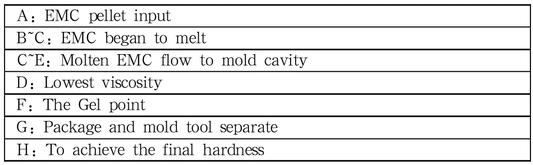
Figure.2 Transfer pressure change during molding
(2)Excellent electronic properties and good mechanical strength,good resistance to chemical corrosion.
(3)Small molding shrinkage.
(4)There is a certain resistance to radiation,moisture resistance,and high temperature resistance.
(5)Low cost.
But EMC molding also can produce some defect such as large wire sweep.Wire sweep is the key response of molding process,large wire sweep will lead to wire touch,and then cause electrical failure potentially.During molding process,EMC presents molten status,large wire sweep even wire broken will occur under the impact of EMC viscosity and flow rate.Wire sweep can’t be completely eliminated,but can be well controlled and improved by optimized molding parameters.
2 The realization of molding wire sweep improvement
To improve wire sweep performance,we need analyze the impact factors of wire sweep.A Mathematical model can present the relationship between EMC viscosity and flow rate with wire sweep.We assuming that the molten EMC is an ideal fluid, the impact(1)F=K**υ*Sin Q.“K”is the constant,“”is the EMC melt viscosity,“υ”is the EMC flow rate (controlled by transfer speed),“Q”is the angle between EMC flow direction and wire.From the formula,the bigger,υ and Q,the bigger F,then the large wire sweep will occurred.[1]Q is fixed by wire looping and gate position on mold tooling;is a process variable.According to the curve graph of EMC viscosity change during molding(See Figure.1), there is a change process from high to low to high for the melt viscosity of EMC and maintains a low viscosity period.So choose a reasonable transfer speed to make sure the EMC fill the mold cavity during a low viscosity.At the same time, flow rate υ also is controlled by transfer speed.
Upon above,we selected SOIC 32EP product Canvas which has longest wire at package corner to perform half shot to define the optimized transfer speed and transfer position distribution.The large wire sweep for Canvas occurred in the last row along the compound flow direction.[2],[3]After mapping,all risk units were located in the fixed position on strip (marked with red) along the compound flow direction, and risk wires are fixed on unit.The mechanism is that the transfer pressure and compound viscosity is highest at this area.(See Figure.2 and Figure.3).
A:EMC pellet input
B~C:EMC began to melt
C~E:Molten EMC flow to mold cavity
D:Lowest viscosity
F:The Gel point
G:Package and mold tool separate
H:To achieve the final hardness
To improve Canvas large wire sweep issue,we need to find the reasonable transfer step distribution by half shot experiment.The analysis is shown as below base on formula (1) and Figure.1 and Figure.3.
1.Reasonable transfer step distribution can prevent the risk wire from high EMC melt viscosity and flow rate especially on risk position of the strip(such as Canvas risk position is 4th row).
2.3 levels for transfer speed,High level(4~6mm/s),Medial level(3~4mm/s),and Low level(1~2 mm/s)was defined.
After performed half shot experiment (See Figure.4), we got the transfer step distribution as below:
Transfer step 1: From the half shot experiment, compound will be filled the 1st row at the transfer position -23mm.In this area, EMC has the low melt viscosity in risk wire with high level transfer speed.So we set transfer position from start position to -23mm and transfer speed 5mm/s as the transfer step1.
Transfer step 2: From the half shot experiment, compound will be filled in half of the 4th row at the transfer position -11mm.In this area, EMC has the various melt viscosity (From low to medium) in risk wire with Medium level transfer speed.So we set transfer position from -23mm to -14mm (keep the 4th row is unfilled completely) and transfer speed 3mm/s as the transfer step2.
Transfer step 3: From the half shot experiment, compound will be filled in the 4th row completely at the transfer position -5mm.In this area, compound viscosity is highest,and high transfer speed also cause wire sweep.So set transfer speed in Low level to fill the cavity smoothly.
According to half shot experiment,we optimized mold parameter as below items (See Figure.5),then collect 30units wire sweep for each setting on risk wire (See Figure.6).
3 Conclusion
The optimized mold parameter has been implemented on Canvas product.After implementation,wire sweep of Canvas is stable and in well controlled(See Figure.7).So this is a valid solution to optimize mold parameter and improve wire sweep performance.
References
[1]Sun Zhongxian,“Epoxy molding compound”,Electronic chemicals,Chemical industry press,2000.
[2]McKennaa,K.P.,& Blumbergerb,J.(2015).First principles modeling of electron tunneling between defects in m-HfO2.Microelectronic Engineering,vol.147,pp.235-238.
[3]Sushko,P.V.,Mukhopadhyay,S.,Stoneham, A.M.,& Shluger,A.L.(2015).Oxygen vacancies in amorphous silica:structure and distribution of properties.Microelectronic Engineering,vol.80,pp.292-295.
