Schottky Barrier Diode Based on Super-Junction Structure
2015-10-14MAKuiYANGFashunandFUXinghua
MA Kui, YANG Fa-shun, and FU Xing-hua
Schottky Barrier Diode Based on Super-Junction Structure
MA Kui, YANG Fa-shun, and FU Xing-hua
(Department of Electronics, Guizhou University; Guizhou Provincial Key Lab for Micro-Nano-Electronics and Software Guiyang 550025)
The contradiction between higherreverse breakdown voltageand lower conductionresistance is important forpower semiconductor devices. Using Super-Junction structure as the voltage support layer can weaken this contradiction. In this paper, a super-junction Schottky barrier diode (SJ-SBD), in which a SJ structure was used as the voltage support layer, was designed and fabricated. The SJ layer which is composed of alternant P-pillar and N-pillar was formed through four times N-type epitaxy and four times P-type implant. SJ-SBD and traditional SBD With the same thickness of drift layer were implemented. And the impurity concentration of P-pillar and N-pillar in SJ layer was the same as that of the drift layer in SBD. The tested results showed that the maximum reverse breakdown voltages are 110 V for traditional SBD and 229 V for SJ-SBD. It is indicated that using the SJ structure as the drift layer could increase thereverse breakdown voltageand reduce the conductionresistance obviously. And the breakdown voltage of SJ-SBD was the maximal when totalcharge inN-pillar and P-pillarwas equal.
breakdown voltage; conductionresistance; Schottky barrier diodes; super-junction
Introduction
SBD is the so called unipolar device since its forward current is attributed to the transportation of majority carriers. It has characteristics such as fast reverse recovery time, high switch speed, and low power consumption. The reverse recovery time of an SBD can be as small as a few nanoseconds. And its on-voltage is about 0.1~0.3 V lower than that of corresponding PN junction devices. Generally, SBDs can be used in high frequency, low voltage, and large current situations[1]. They can also be used as freewheel diodes and protected diodes. Deliberated designed SBDs are used as ultra high frequency rectifier diodes and small signal detector diodes in microwave communication[2-3].
The basic requirements for a rectifier device are higher current capacity, lower conduction loss, higher transient speed, and higher reverse breakdown voltage. For SBD, the resistance of the drift layer is a major component of the on-resistance, and this layer mainly supports the reverse voltage. On the one hand, the drift layer should be thinner and heavily doped to make sure that the on-resistance is small enough. On the other hand, higher reverse breakdown voltage needs a thicker drift layer with lighter doping. Therefore, we must compromise the thickness and doping concentration of the drift layer of an SBD to balance the on-resistance and the reverse breakdown voltage. In this paper, the Super-Junction structure which is composed of alternate P-pillar and N-pillar[4]was used to replace the drift layer to alleviate the contradiction between low on-resistance and high reverse breakdown voltage. The Super-Junction structure was fabricated through four times N-type epitaxy and four times P-type implant. The diode with super-junction structure is called SJ-SBD[5-6]. The geometric parameters and process parameters of the proposed SJ-SBD were optimized through simulation under the SILVACO platform. The reverse breakdown voltage of the fabricated SJ-SBD is about 100 V higher than that of the traditional SBD.
1 Design of the SJ-SBD
A traditional SBD consists of a heavy doped substrate, a lightly doped epitaxial layer, and a metal-epitaxial layer Schottky contact. When the diode is forward biased, the resistance of the lightly doped epitaxial layer is the major component of the on-resistance. When it is reverse biased, the lightly doped epitaxial layer mainly supports the reverse voltage. The relationship between the on-resistanceonand the reverse breakdown voltagePP[7]is:
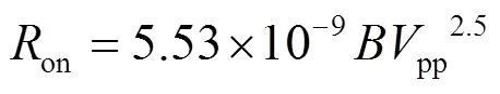
This equation is the well known “silicon limit”. It shows that there is contradiction between low on-resistance and high reverse breakdown voltage for SBDs.

Compared with equation (1), the contradiction between low on-resistance and high reverse breakdown voltage was alleviated obviously.
a. 2-D structure b. the SJ cell
Fig.1 Basic structure of SJ-SBD
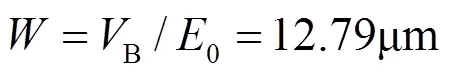
The specification of an SJ-SBD is 200 V of breakdown voltage and 0.9 V of on-voltage under 10 A current. By using a quasi 2-D model, the relationship between the maximum electric field0and reverse voltageBcan be expressed as[9-10]:

whereis the horizontal size of SJ cell,is the thickness of the SJ layer, andp,nare the fit parameters for optimization for the P-pillar and N-pillar respectively.
By usingB=220 V,/=2.5, andp=n=16.1,0=1.72105Vcm, the thickness of SJ layer can be expressed as:
For interdigitated SJ cell, the optimized design isN=P=andSJ=a=d, whereNandPare the width of the N-pillar and the P-pillar, respectively,dandaare the doping concentration of the N-pillar and the P-pillar, respectively, andN=P=5.116 µmis then determined.
The relationship between the electric field and doping concentration in N-pillar[9, 11]is:
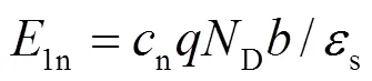
Wheresis the dielectric constant of silicon,is the electron charge, andnequals 0.371 for inter-digital SJ cell. By usingn,,0,s,and equation (5), the doping concentration of N-pillar isd=5.8×1015cm-3. Using the same method, the doping concentration of P-pillar can be solved asa=5.8×1015cm-3.
The actual parameters should be larger than the calculated values to tolerate process variations. So, the thickness of the SJ layer was designed for 14 µm and the doping concentration of both N-pillar and P-pillar were designed for 6×1015cm-3. In order to analyze the influence of the quantity of charge in N-pillar and P-pillar on the reverse breakdown voltage of SJ-SBD, we designed three kinds of SJ structures. The width of N-pillar and P-pillar wereN=P=6 µm,N=6 µm andP=10 µm,N=10 µm andP=6 µm, respectively.
2 Simulation and Analysis
Fig.2 shows the 2-D structure of traditional SBD and the proposed SJ-SBD simulated in process simulation tool ATHENA. Both of them consist of a heavily doped substrate, a light doped drift layer, and a Schottky contact formed by depositing PtSion the drift layer. The difference between these two SBDs is that the drift layer in SJ-SBD is a SJ layer which was formed through four times N-type epitaxy and four times P-type implant. After the completion of all process steps, the impurity concentration of P-pillar and N-pillar in the SJ layer is same as that of the drift layer in SBD. Moreover, the top of P-pillar is necessarily heavily doped to make sure a good ohmic contact between P-pillar and PtSi.
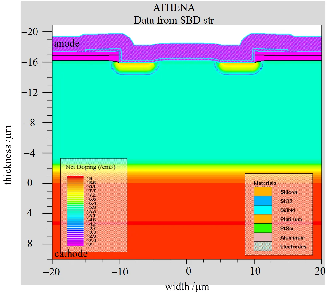
a. 2-D structure of traditional SBD
b. 2-D structure of SJ-SBD
Fig.2 2-D structure of two SBDs
Electrical characteristics of these two diodes were simulated in the device simulation tool ATLAS. The simulated result indicated that the on-voltage is about 0.7 V. The electric field distribution in case of reverse breakdown and characteristic curve under reverse bias are shown in Fig.3. In the SJ structure, chargecompensation occured between P-pillar and N-pillar interactively under reverse bias. And the whole SJ layer would be depleted completely when the device is breakdown. From Fig.3aandFig.3b, we can see that the depletion layer in SJ-SBD is much thicker than that in SBD under reverse breakdown situation. So, the breakdown voltage of SJ-SBD must be higher than that of traditional SBD obviously. Fig.3c shows the characteristic curve under reverse bias. It indicates that the breakdown voltage of SJ-SBD is higher about 120 V than that of traditional SBD.
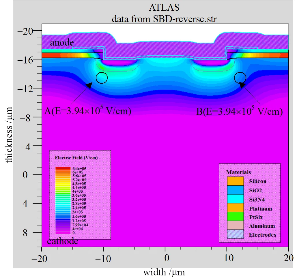
a. distribution of electric field under breakdown for SBD
b. distribution of electric field under breakdown for SJ-SBD
c. characteristic curve under reverse bias
The SJ layer can improve the reverse breakdown voltage of the SJ-SBD, but many parasitic PN junctions will be formed in the drift layer, which is not only the reverse voltage support layer, but also the region where forward current flows through. These PN junctions increase the parasitic capacitance, and they are also forward biased when the SJ-SBD is forward biased. when the SJ-SBD turns off, the recombination of minority carriers which exist near the boundary of the space charge region of these parasitic PN junctions takes a long time. So, the high frequency response of the SJ-SBD goes bad. The simulated reverse recovery characteristic curves of traditional SBD and SJ-SBD are shown in Fig.4. From these two curves, we can see that the reverse recovery time of SJ-SBD is observably longer than that of traditional SBD when forward current of two devices is equal.
3 Fabrication and Test Results
The proposed SJ-SBD consisted of a heavily doped N-type substrate, an SJ layer, and a Schottky contact. Firstly, an N-type epitaxial layer with a thickness of about 1/4 designed SJ layer (in Fig.1) was prepared on the start substrate. Then P type dopant was implanted in the place where to form P-pillar. This process four times was repeated and the sample in proper temperature and time was annealed. The SJ structure with N pillar and P pillar were then formed as shown inFig.2b. Subsequently, the top of P-pillar was heavily doped. After the deposition of PtSi, an ohmic contact between P-pillar and metal anode and Schottky contact between N-pillar and metal anode were formed. The fabrication of SJ-SBD chip was finally completed.
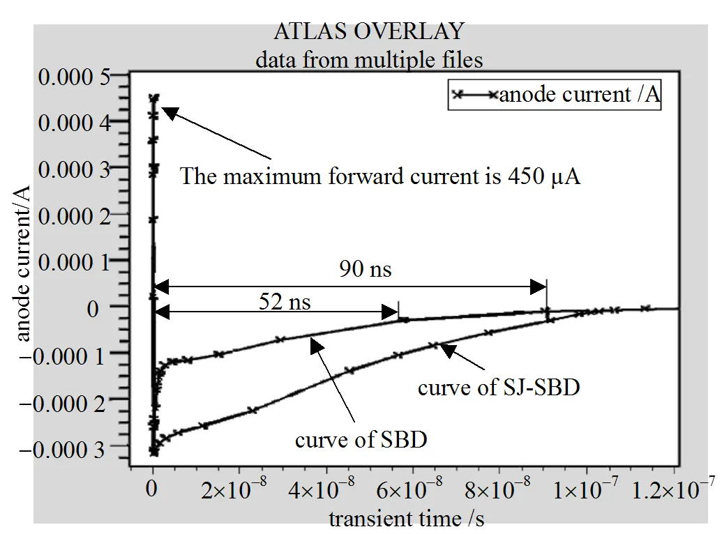
Fig.4 Reverse recovery characteristic curves of the SJ-SBD and traditional SBD
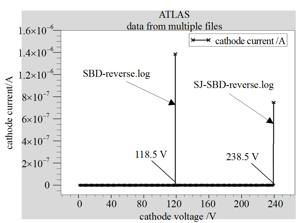
A traditional SBD with the same thickness and doping concentration of drift layer was fabricated at the same time. Fig.5shows the tested breakdown voltage curves of two SBDs. We can see that the breakdown voltage of traditional SBD is about 110 V from Fig.5a, and about 229 V of SJ-SBD from Fig.5b.

a. traditional SBD
b. SJ-SBD
Fig.5 Tested results of reverse breakdown characteristic curves of SBD and SJ-SBD
Electric characteristics of the fabricated SBDs were tested in the semiconductor testing system (351-GT/P). Tested results are listed in table.1. The tested results in table.1 indicate that breakdown voltages of SJ-SBDs are higher than that of traditional SBD. On-voltage and inrush current of these two kinds of SBDs are nearly equal. Reverse current of traditional SBD is lower than that of SJ-SBDs. The relatively higher reverse current of SJ-SBDs is caused by the parasitic PN junctions composed of alternate P-pillar and N-pillar in the SJ structure. Reverse recovery time of SJ-SBDs is obviously longer than that of the traditional SBD. The reason is that the SJ structure in SJ-SBDs makes minority carriers contribute to forward current and increase the parasitic capacitance.
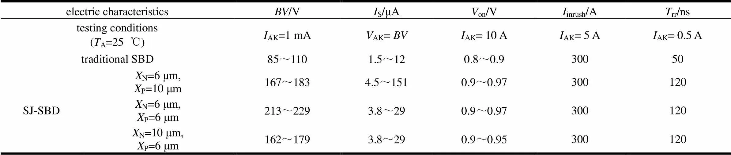
Table. 1 Tested electric characteristics of the fabricated SBDs
PS:Nis the width of N-pillar,Pis the width of P-pillar
High breakdown voltage of SJ structure profits from the same charge quantity in N-pillar and P-pillar. If the charge quantity in these two areas is different, the breakdown voltage of this layer will be significantly reduced. From the tested results in table.1, we can conclude that a symmetric structure of N-pillar and P-pillar will have higher breakdown voltage.
4 Summary
The reverse breakdown voltage of the fabricated SJ-SBD is about 100 V higher than that of the traditional SBD for the same thickness and doping concentration of the N-type drift layer. The results indicate that for the proposed SJ-SBD, the lightly doped epitaxial layer for reverse voltage supporting can be replaced by alternate N and P pillars (SJ-structure), where a higher dopant concentration can be adopted to reduce the on-resistance while keeping a rather high breakdown voltage. Using the SJ layer as the reverse voltage support layer can alleviate the contradiction between low on-resistance and high reverse breakdown voltage. But the PN junctions composed of alternate P-pillars and N-pillars in the SJ structure cause higher reverse current and longer reverse recovery time.
We would like to acknowledge the Dr. fund of Guizhou university [Gui da Ren Ji He Zi (2013) 20Hao], which partly supported this work.
[1] Fatima Z M, Luca V, SHIKTOROV P, et al. High- frequency voltage noise of nanometric schottky-barrier diodes and heterostructure barrier varactor in cyclostationary conditions[C]//21st International Conference on Noise and Fluctuations (ICNF). Toronto: [s.n.], 2011: 216-219.
[2] ÇETINKAYA H G, TECIMER H, USLU H, et al. Photovoltaic characteristics of Au/PVA (Bi-doped)/n-Si Schottky barrier diodes (SBDs) at various temperatures[J]. Current Applied Physics, 2013, 13(6): 1150-1156.
[3] GRAFFEUIL J, LIMAN R A, MURARO J L, et al. Cyclostationary shot-noise measurements in RF Schottky-barrier diode detectors[J]. IEEE Electron Device Letters, 2010, 31(1): 74-76.
[4] FUJIHIRA T. Theory of semiconductor super junction devices[J]. Jpn J Appl Phys, 1997, 36(10): 6254-6262.
[5] MUSUMECI S, PAGANO R, RACITI A, et al. Modeling and characterization of a merged PiN Schottky diode with doping compensation of the drift region[C]//IAS.seattle: [s.n.], 2004: 1244-1251.
[6] WANG Ying , XU Li-kun , MIAO Zhi-kun . A superjunction Schottky barrier diode with trench metal–oxide– semiconductor structure[J]. IEEE Electron Device Letters. 2012, 33(12): 1744-1746.
[7] BALIGA B J. Modern Power Device[M].New York:John Wiley& Sons. 1987: 269-276.
[8] CHEN X B, JOHNNY K O S. Optimization of the specific on-resistance of the COOLMOSTM[J]. IEEE Transactions on Electrons Devices, 2001, 48(2): 344-348.
[9] CHEN X B. Theory of a novel voltage-sustaining composite buffer(CB) layer for power devices[J]. Chinese Journal of Electronics, 1998(7): 211-216.
[10] CHEN Xing-bi. Optimum design parameters for different patterns of CB-structure[J]. Chinese Journal of Electronics, 2000, 9(1): 6-10.
编 辑 张 俊
基于超结结构的肖特基势垒二极管
马 奎,杨发顺,傅兴华
(贵州大学电子科学系;贵州省微纳电子与软件技术重点实验室 贵阳 550025)
在功率半导体器件中,高的反向击穿电压和低的正向导通电阻之间的矛盾关系是影响其发展的主要因素之一,选用超结结构替代功率半导体器件中的传统电压支持层能够有效缓解这一矛盾关系。该文设计和实现了一种超结肖特基二极管,其中的电压支持层采用P柱和N柱交替构成的超结结构。在器件的制作方面,选用成熟的单步微电子工艺,通过4次N型外延和4次选择性P型掺杂来实现超结结构。为便于对比分析,设计传统肖特基二极管和超结肖特基二极管的电压支持层厚度一致,且超结结构中P柱和N柱的杂质浓度均和传统肖特基二极管的电压支持层浓度一致。测试得到传统肖特基二极管的反向击穿电压为110 V,而超结肖特基二极管的反向击穿电压为229 V。表明采用超结结构作为功率半导体器件的电压支持层能够有效提高反向击穿电压,同时降低器件的正向导通电阻,并且当P柱区和N柱区内的电荷量一致时器件的击穿电压最高。
击穿电压; 导通电阻; 肖特基势垒二极管; 超结
TN311+.8
A
2013-01-17;
2014-10-28
国家自然科学基金(61464002); 贵州省工业攻关项目(黔科合GY字[2009]3026); 贵州省科学技术基金(黔科合J字[2011]2203; 黔科合J字[2014]2066)
2013-01-17; Revised date:2014-10-28
supported by NSFC(61464002); Industrial Research Projects in Guizhou Province (Qian Ke He GY Zi [2009]3026); Science and Technology Fund of Guizhou Province (Qian Ke He J Zi [2011]2203, Qian Ke He J Zi [2014]2066); Dr. Fund of Guizhou University (Gui Da Ren Ji He Zi (2013)20Hao)
10.3969/j.issn.1001-0548.2015.01.023
Biography: MA Kui, born in 1985, male. associate professor, Research interesting:analog ICs, power semiconductor devices and power ICs.
马奎(1985-),男,副教授,主要从事模拟集成电路、功率半导体器件和功率IC方面的研究.