Optimal Control Strategy for Buck Converter Under Successive Load Current Change*
2014-04-24FangWei方炜LiuXiaodong刘晓东LiuYanfei刘雁飞
Fang Wei(方炜),Liu Xiaodong(刘晓东),Liu Yanfei(刘雁飞),2
1.Key Lab of Power Electronics and Motion Control,Anhui University of Technology,Ma′Anshan,243002,P.R.China;2.Queen′s University,Kingston K7L3N6,Canada
1 Introduction
In modern dc-dc switch mode power supplies,the tight voltage regulation and fast response to load change are among the most important requirements[1].A larger output filtering capacitor is always used to reduce output voltage derivation,however,this will occupies more board area and increase the cost.Thus,without modifying the hardware,couples of analog controllers and digital control algorithms have been developed in some previous literatures to improve the dynamic response of the dc-dc converters.Analog control strategies such as V2and hysteretic control,have received extensive attention in recent years,however,the main application challenge is the variations of the converter switching frequency[2-3].Considering the intrinsic nonlinear nature of the switched regulators,various nonlinear methods have been introduced to achieve fasttransient responses to load-step events.In Ref.[4],the state plane of the dc-dc converter was partitioned by means of one or more switching surface,and a nonlinear sliding-mode controller was presented to drive the state trajectory rapidly converged to the regulation point.Since the selection of the switching surfaces is a central problem in the boundary-control theory,several design criteria and comparative studies regarding the choice of the switching surfaces have been proposed[5-6].In Ref.[7],by using an 8-bit microcontroller,a self-regulating fuzzy control scheme was presented for the forward dc-dc converters.In Ref.[8],based on the Takagi-Sugeno model,the stability and performance was analyzed for the Boost converter which was controlled by a nonlinear fuzzy controller.
Although these approaches presented in the literatures differ with varying performance in terms of speed and robustness,they cannot achieve a faster response to load current disturbance.In Refs.[9,10],some digital optimal schemes are discussed for dc-dc converters to approximate the fastest transient response during a transient event.In Ref.[11],by using the principle of capacitor charge balance control(CBC),a digital controller predicts the minimum voltage overshoot/undershoot and the recovery time for a buck converter.But it requires a sampling delay and complex mathematical computation.Based on the principle of CBC,couples of analog controllers and digital control algorithms were reported to improve the dynamic response of other power converters(such as the Boost converter,the Buck-Boost converter)in Refs.[12,13].However,these controllers only considered one-step load current change,and the algorithm required the condition that load current should keep constant during a transient.Consequently,the CBC controller is unsuitable for a successive load-change.
A new digital control algorithm is discussed in this paper for dc-dc converters to enhance the dynamic performance during a successive loadchange condition.Under a steady-state condition,the output voltage is tightly regulated by a digital voltage mode controller(VMC).Once the load current change is significant,an optimal control scheme is activated immediately.With the integration of the capacitor current,the proposed CBC algorithm predicts the switching time based on the charge balance control,and the optimal transient performance under a successive loadchange is thus achieved.Compared with a conventional proportion integration differentiation(PID)controller,the proposed algorithm provides much better dynamic performance.
2 Principle of CBC Algorithm
The dc-dc Buck converter,composed of switchers Q1,Q2,an output filter circuit and a load R,is considered in this paper(Fig.1).
According to the algorithm of capacitor charge balance,the average value of capacitor current over transient time must be equal to zero under one-step load current change[11].
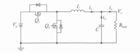
Fig.1 SR-Buck converter
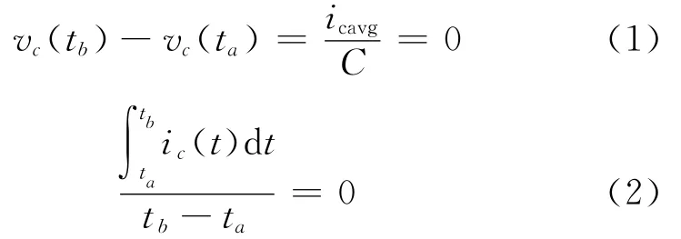
where ta,tbare the beginning time and the end time of the transient period,respectively;ic,vcthe current and the voltage of the output capacitor,respectively;Cthe value of the output capacitor.When Eq.(2)is satisfied,it means that the output voltage returns to the reference voltage after a transient period.Furthermore,if the inductor current iLequals to the new load current at time tb,the SR-Buck converter has recovered from a transient event(Fig.2).
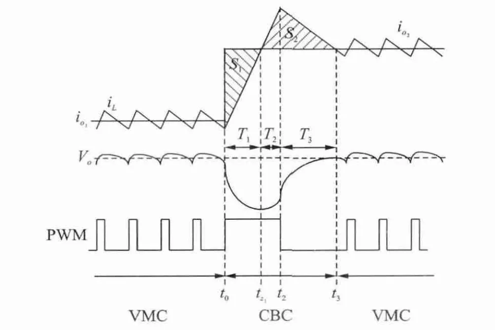
Fig.2 Optimal dynamic response of Buck converter under positive load-current change
3 Mathematical Analysis of the Proposed Algorithm
In Fig.2,the whole transient period under one-step load current change can be divided into two parts,i.e.,one part that the capacitor supplies a portion of the load current before tz1and the other part that the capacitor begins recharge before t3.In other words,the two parts determine the discharge portion(S1)and the recharge portion(S2).It should be noted that the capaci-tor current crosses zero at tz1,which is regarded as the turning point in the transient period.Once tz1is obtained,the discharge portion of the capacitor can be calculated directly.Thus,the key point of the CBC algorithm is to accurately obtain the value T1(determined by tz1),therefore,the charge of the capacitor keeps balance at the end of a transient period.
Before the introduction of the proposed algorithm,some assumptions should be considered,that is,
(1)the ESR and ESL can be neglected;
(2)the values of the inductor and capacitor keep constant;
(3)the input voltage keeps unchanged during the transient.
3.1 One-step load-current change
Firstly,the rising and falling slew rate of the inductor current is given as

Based on Fig.2,the discharge portion S1can be calculated as

while the charge portion S2can be given as
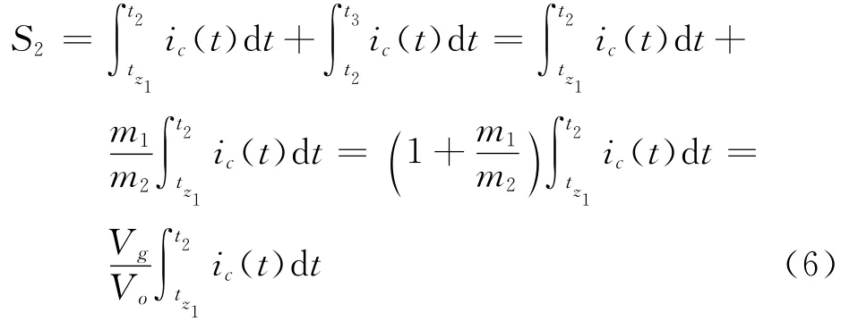
According to the principle of the CBC,at the end of transient,the following equations should be fulfilled

Thus,the optimal transient time T1,T2and T3can be given by

A similar analysis can be performed for a negative load step based on Fig.3.The following equations should be satisfied

Moreover,the optimal transient time T1,T2and T3under a negative load step change can be obtained

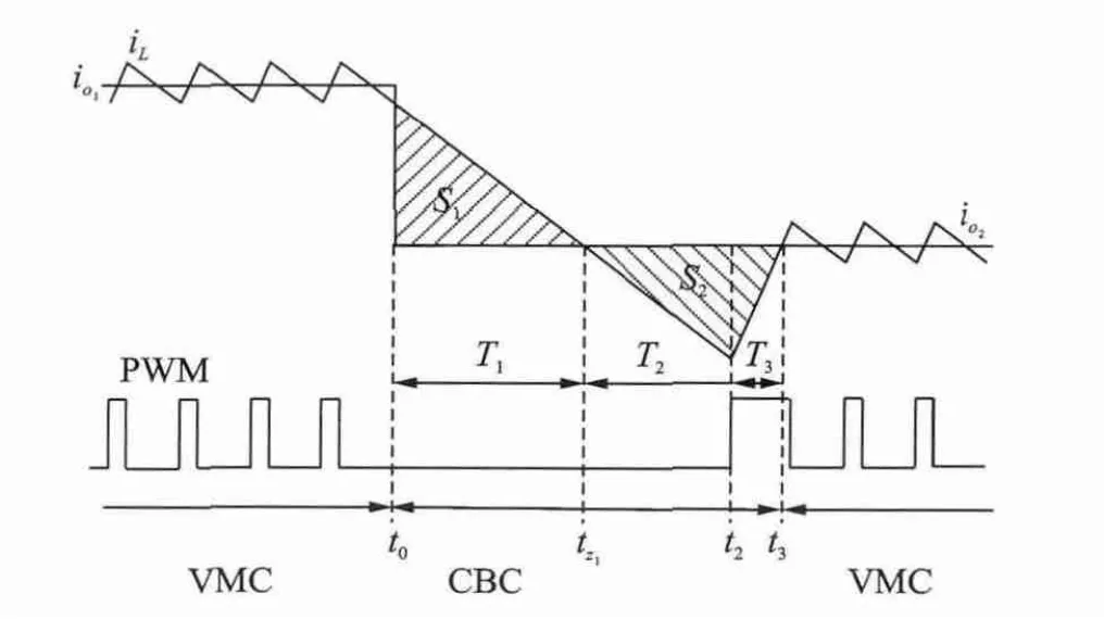
Fig.3 Optimal dynamic response of Buck converter under negative load-current change
3.2 Successive load-current change
If a successive positive load-current change is considered,the proposed algorithm executes the corresponding action according to the different step change,as shown in Figs.4(a,b).It is obvious that the response is more complicate than that of the one-step load change.It is divided into several parts,including the discharge portion(S1,S3)and the recharge portion(S2,S4)in Fig.4.However,the detection of the point(tz1and tz2)is still the key step in the proposed algorithm,because the capacitor turns into the recharge portion at tz1and tz2.
According to the algorithm of the capacitor charge balance control,at the end of transient,the following equation should be fulfilled

It should be noted that the recharge portion S4can be calculated similarly to the one-step load change
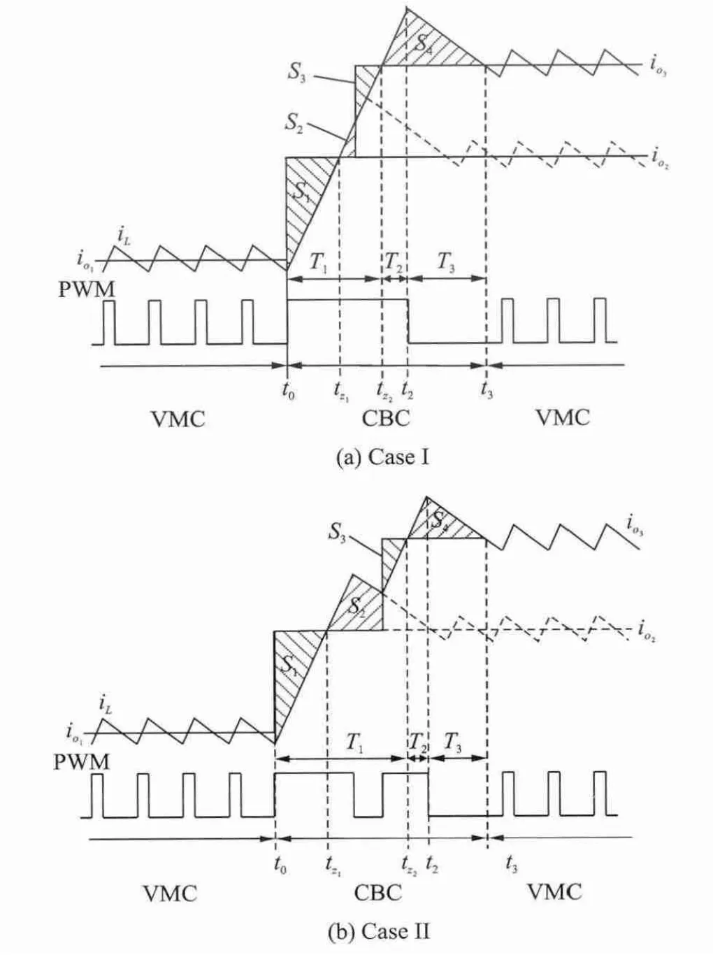
Fig.4 Optimal dynamic response of Buck converter under successive positive load current change
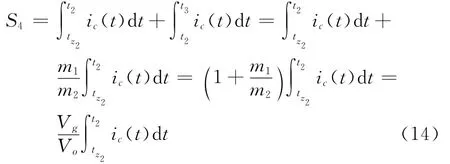
Moreover,the sum of the portions S1,S2,S3can be given directly by the integration of the capacitor current over the period[t0tz2]

Substituting Eqs.(14,15)into Eq.(13)yields

In Fig.5,the optimal transient time T1,T2and T3can be calculated as

A similar analysis can be carried out for a negative load step based on Fig.5.The following equation should be fulfilled

Then the optimal transient time has the following expression

With some minor change to Eqs.(16—19),the same analysis can be applied to the dc-dc converter under other successive load change conditions,which will not be discussed in this paper.
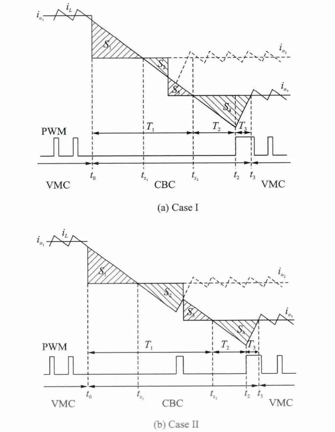
Fig.5 Optimal dynamic response of Buck converter under a successive negative load current change
4 Implementation of the Proposed Digital Controller
4.1 Outline of algorithm operation
According to the analysis in Section 3,the key steps of the proposed algorithm can be listed as follows:
(1)After detecting a load current change(by comparing the change of the load current iowith the predefined threshold),the optimal control scheme is activated immediately at t0,and the counter and the integration of the capacitor current icin the digital controller are triggered;
(2)The duty cycle is set as the maximum value 100%(apositive step change)or the minimum value 0%(a negative step change),which drives the induct current iLrise or fall at its maximum slew rate;
(3)Once Eq.(8)or Eq.(11)is fulfilled,which means iLreaches its peak value or valley value(at t2in Figs.2,3),the duty cycle is set to 0%(apositive step change)or 100%(a negative step change);
(4)If a successive load change occurs(by comparing the iochange with the threshold),the duty cycle is reset as 100%or 0%again,as shown in Figs.4,5;
(5)When the condition of the charge balance control is satisfied,the digital controller returns to the conventional digital PID control scheme again.
4.2 Hardware implementation
The hardware implementation diagram of the proposed charge balance control algorithms is shown in Fig.6.RLand Roare the high precision resistances used to sample the inductor current and the load current.Cv-sens,CiL-sensand Cio-sensare the decoupling capacitor of the operational amplifiers.
4.3 Digital controller based on FPGA
In Fig.7,the proposed algorithm is programmed by Block diagram method in FPGA,with the logic elements(4,429),registers(2,848)and memory bits(251,560).
In Fig.7,the clock module products the clock signals,which are used in other modules and A/D sample.The digital PID module is constructed according to the following equation

where the coefficients are given as

where Kp,τi,τdare the parameters of the PID controller.Tis the sample period.
The proposed algorithm is programmed in the CBC module,including several submodules,such as the load step detection,the crossing-zero judgment of the ic,and the charge balance control(Fig.7).
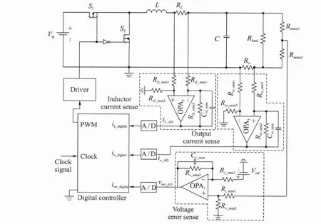
Fig.6 Hardware implementation diagram

Fig.7 Block diagram implementation of the proposed algorithms in FPGA
5 Simulation and Experiment Results
To verify the performance of the proposed method,a Buck converter,undergoing several successive load current changes,was proposed.The parameters of the converter were provided as follows:Vin=5V,Vo=1.5V,fs=250kHz,L=1.5μH,C=290μF.
5.1 Simulation results
Simulation is performed by Matlab/Simulink.For comparison,a well-designed digital PID controller with bandwidth of 30kHz and phase margin of 52°is also simulated.

Fig.8illustrates the different dynamic performance of the Buck converter under a PID controller and a CBC controller,while a positive successive load step change(from 0Ato 5Ato 10A).It is observed that,by using the PID controller,the undershoot of the output voltage is 102mV and the recovery time is 81μs;while using the proposed CBC algorithm,the overshoot is reduced to 15mV and the settling time is reduced to 11μs,which are improved by 85%and 86%,respectively,compared with those of the PID controlled converter.
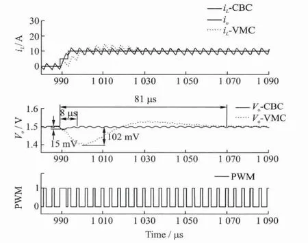
Fig.8 Simulation results of output voltage response to apositive successive load current change(0A→5A→10A)
For a negative successive load step change(from 10Ato 5Ato 0A),as shown in Fig.9,with the proposed controller,the overshoot is reduced to 21mV,which is improved by 76%,and the settling time is reduced to 12μs,which is improved by 84%,compared with those of the PID controlled converter.
Simulation results demonstrated that the settling time of the converter with the proposed algorithm is improved significantly compared to that of the PID controlled converter.
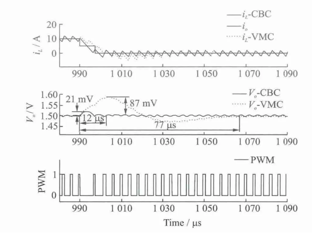
Fig.9 Simulation results of output voltage response to an negative successive load current change(10A→5A→0A)
5.2 Experimental results
An experimental prototype of a Buck converter was designed and implemented with FPGA by using the aforementioned algorithm.
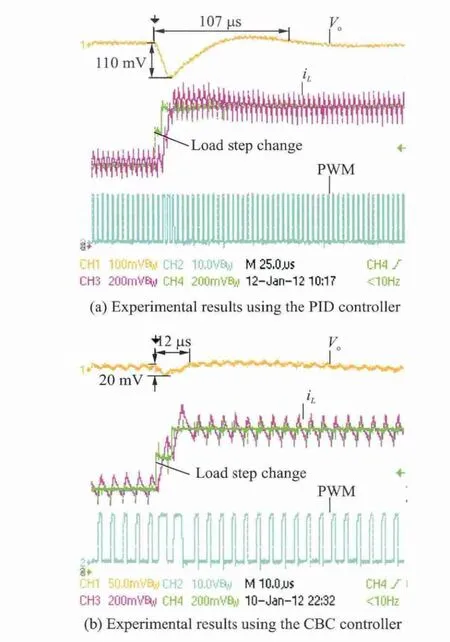
Fig.10 Experimental results of successive positive load transient case 0A→5A→10A
In Fig.10(a)and Fig.11(a),the experimen-tal results illustrate the transient performance of the PID controller under the successive load step change between 0Aand 10A.Limited by the bandwidth,the voltage mode controller has large voltage variations and long recovery time.For a positive load transient,the undershoot voltage is about 110mV with 107μs settling time.While,the overshoot voltage is 120mV with 118μs settling time during a negative load transient.
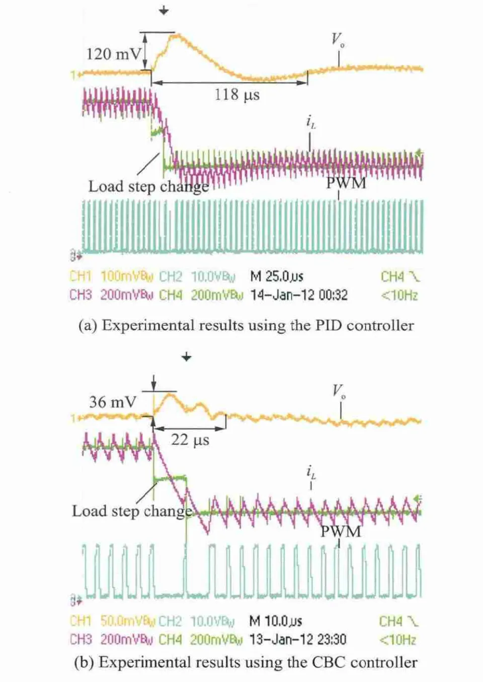
Fig.11 Experimental results of successive negative load transient case 10A→5A→0A
Experimental results of the proposed CBC controller under the load step change between 10Aand 0Aare shown in Fig.10(b)and Fig.11(b).Compared to the PID controller,the undershoot voltage is reduced by 81%with the recovery time shortened by 88%for a positive load step change,while the overshoot voltage is reduced by 70%with the recovery time shortened by 81%for a negative load step change.
6 Conclusions
A practical digital control algorithm has been presented for improving the dynamic performance of dc-dc converters under a successive load-change condition.The controller utilizes the principle of the charge balance control,where a PID compensator and a CBC controller are combined to provide the tight output voltage regulation and fast transient response.Furthermore,conditions and equations for capacitor charge balance are derived.The effectiveness of the proposed algorithm is verified on an experimental prototype of a Buck converter,demonstrating stable operation and fast transient response in different operating conditions.
[1] Zhong Jie,Yu Shenglin,Liu Shousheng.Simulation study of chaos in DC-DC converter[J].Transactions of Nanjing University of Aeronautics and Astronautics,2003,20(1):79-84.
[2] Huerta S C,Alou P,Garcia O,et al.Hysteretic mixed-signal controller for high-frequency DC-DC converters operating at constant switching frequency[J].IEEE Transactions on Power Electronics,2012,27(6):2690-2696.
[3] Liu Jun,Yan Yangguang.Reliable hysteresis current controlled dual buck half bridge inverter[J].Transactions of Nanjing University of Aeronautics and Astronautics,2003,20(1):67-72.
[4] Siew-Chong T,Lai Y M,Tse C K.General design issues of sliding-mode controllers in DC-DC converters[J].IEEE Transactions on Industrial Electronics,2008,55(3):1160-1174.
[5] Rong-Jong W,Li-Chung S.Design of voltage tracking control for DC-DC boost converter via total sliding-mode technique[J].IEEE Transactions on Industrial Electronics,2011,58(6):2502-2511.
[6] Lam H K,Tan S C.Stability analysis of fuzzy-model-based control systems:application on regulation of switching DC-DC converter[J].IET Control Theory and Applications,2009,3(8):1093-1106.
[7] Hsu C F,Chung I F,Lin C M,et al.Self-regulating fuzzy control for forward DC-DC converters using an 8-bit microcontroller[J].IET Power Electronics,2009,2(1):1-12.
[8] Mehran K,Giaouris D,Zahawi B.Stability analysis and control of nonlinear phenomena in boost converters using model-based Takagi-Sugeno fuzzy approach[J].IEEE Transactions on Circuits and Systems,2010,57(1):200-212.
[9] Wen Y,Trescases O.DC-DC converter with digital adaptive slope control in auxiliary phase for optimal transient response and improved efficiency[J].IEEE Transactions on Power Electronics,2012,27(7):3396-3409.
[10]Cortes P,Quiroz F,Rodriguez J.Predictive control of a grid-connected cascaded H-bridge multilevel converter[C]//Proceedings of the 2011-14th European Conference on Power Electronics and Applications,EPE,2011:1-7.
[11]Feng G,Meyer E,Liu Y F.A new digital control algorithm to achieve optimal dynamic response performance in DC-to-DC converters[J].IEEE Transactions on Power Electronics,2007,22(4):1489-1498.
[12]Liu X D,Ge L,Fang W,et al.An algorithm for Buck-Boost converter based on the principle of capacitor charge balance[C]//2011 6th IEEE Conference on Industrial Electronics and Applications,ICIEA.[S.l.]:IEEE,2011:1365-1369.
[13]Fang W,Qiu Y J,Liu X D,et al.A new digital capacitor charge balance control algorithm for Boost DC/DC Converter[C]//2010IEEE Energy Conversion Congress and Exposition,ECCE. [S.l.]:IEEE,2010:2035-2040.
猜你喜欢
杂志排行
Transactions of Nanjing University of Aeronautics and Astronautics的其它文章
- Predictive Modeling and Parameter Optimization of Cutting Forces During Orbital Drilling*
- Wear Behaviour of Electroless Ni-P-Diamond Composite Coatings*
- Method for Measuring Residual Stresses Induced by Boring in Internal Surface of Tube and Its Validation with XRD Method*
- Theoretical and Experimental Investigation of Laser Milling Assisted with Jet Electrochemical Machining*
- Structural Design and Control Strategy Analysis of Micro/Nano Transmission Platform*
- Friction and Wear Properties of Amorphous Carbon Nitride Coatings in Water Lubrication*
