Design of data transmission for a portable DAQ system
2014-04-24ZHOUWenXiong周文雄WANGYanYu王彦瑜NANGangYang南钢洋andZHANGJianChuan张建川
ZHOU Wen-Xiong(周文雄),WANG Yan-Yu(王彦瑜),NAN Gang-Yang(南钢洋),and ZHANG Jian-Chuan(张建川)
1Institute of Modern Physics,Chinese Academy of Sciences,LanZhou,730000,China
2University of Chinese Academy of Sciences,Beijing,100039,China
Design of data transmission for a portable DAQ system
ZHOU Wen-Xiong(周文雄),1,2WANG Yan-Yu(王彦瑜),1,∗NAN Gang-Yang(南钢洋),1,2and ZHANG Jian-Chuan(张建川)1,2
1Institute of Modern Physics,Chinese Academy of Sciences,LanZhou,730000,China
2University of Chinese Academy of Sciences,Beijing,100039,China
Field Programmable Gate Array(FPGA),combined with ARM(Advanced RISC Machines)is increasingly employed in the portable data acquisition(DAQ)system for nuclear experiments to reduce the system volume and achieve powerful and multifunctional capacity.High-speed data transmission between FPGA and ARM is one of the most challenging issues for system implementation.In this paper,we propose a method to realize the high-speed data transmission by using the FPGA to acquire massive data from FEE(Front-end electronics)and send it to the ARM whilst the ARM to transmit the data to the remote computer through the TCP/IP protocol for later process.This paper mainly introduces the interface design of the high-speed transmission method between the FPGA and the ARM,the transmission logic of the FPGA,and the program design of the ARM.The theoretical research shows that the maximal transmission speed between the FPGA and the ARM through this way can reach 50MB/s.In a realistic nuclear physics experiment,this portable DAQ system achieved 2.2MB/s data acquisition speed.
Field Programmable Gate Array(FPGA),Advanced RISC Machines(ARM),High-speed transmission,Driver, Data acquisition(DAQ)
I.INTRODUCTION
In order to ref l ect the mechanism of nuclear reaction,we have to measure many groups of parameters simultaneously when performing a nuclear physics experiments[1].Even though it is a small nuclear physics experiment,we still need to acquire several parameters due to the relevance of the particles produced by particles collision in accelerator.In order to meet the requirements of the small nuclear physics experiment,a PDAQ(portable DAQ)system based on Field Programmable Gate Array(FPGA)and Advanced RISC Machines(ARM)is developed.In this system,the FPGA is applied to control the FEE(Front-end electronics),and transmit the data converted by ADCs to the ARM.Whilst,the ARM is designed to send the data to the other computer for real-time storing and processing.Considering the maximal DAQ rate of the FEE for this system is 8MB/s,the speed of the data transmission from the FPGA to the ARM must be more than 8MB/s.
In present nuclear physics experiments,many DAQ systems based on CAMAC(Computer Automated Measurement And Control)bus are still used,whose maximal transmission rate is 3MB/s[2].But the bus is not able to meet the need of the PDAQ system for its speed[3].In addition,there are also lots of DAQ systems which are based on VME(VERSA-Module-Eurocard),FASTBUS,PCI(Peripheral Component Interconnect)or PXI(PCI eXtensions for Instrumentation)bus[4].Although the speed of these buses can reach the requirements of the PDAQ system[5,6],it is also not suitable for the PDAQ system.Because the protocols are very complicated and the I/O ports of the ARM are not compatible with those protocols. Besides,some of the portable devices are based on serial bus such as SPI,I2C and so on[7].Due to its speed limitation,itis also not suitable for this system.Thus,we choose the highspeed parallel communication method.Not only because of its simple protocols but also the advantage of low cost and fast speed.Compared to the other methods,it is easier to design and it can fully meet the requirements of the PDAQ system.
There are two important points for this communication method:Firstly,the FPGA is designed as a memory connected to the IO bus of the ARM;Secondly,the FPGA is controlled by the SROM(static read only memory)controller(SROMC) integrated in the ARM.This data communication mechanism can raise transmission rate between the FPGA and the ARM up to50MB/s theoretically.Itcanmeetthedesign requirement of the PDAQ system.In the nuclear experiment,the system is used to obtain energy spectrum of Na22.And the spectrum is the same with that obtained through PHILLIPS7164,which is a CAMAC module.

Fig.1.DAQ System architecture.
II.PDAQ SYSTEM ARCHITECTURE
The system consists of some DAQ modules developed completely in-house.The DAQ module is designed using FPGA and ARM.It can workindependently or together with the other same modules.So it is very convenient to extend the ADC modules for the requirements of a nuclear experiment.Fig.1 shows the architecture of the system.The DAQ module can work in master mode or client mode.The FPGA is used to control 4 local ADCs through ADC-BUS and communicate with the other DAQ modules through Back-BUS.Only in master mode,the DAQ module needs to transmit data to the ARM through SROM-BUS.All of the data is sent to the other computer for processing through Ethernet.
III.COMMUNICATION METHODS BETWEEN THE FPGA AND THE ARM
The communication methods between the FPGA and the ARM include serial communication,custom parallel communication and the high-speed parallel communication[8].The speeds of those communication methods are shown in Table 1.

TABLE 1.The speeds of different communication methods[9]
Owing to the limitations of the protocols and characteristics for the ARM,the serial communication method cannot meet the least requirement of the PDAQ system.For custom parallel communication method,the data and address bus must consist of GPIO ports.A experiment is designed to get the maximal electrical level change rate of the GPIO ports in Linux operation system.It shows that the minimal period of the electrical level change is 5µs.Thus,if the custom data bus width is 16bits,the transmission speed can be calculated through the following formula:

AsW=16bits,andT=5µs,the transmission speed(S)is about 0.4MB/s(tested under Linux operation system).It still can’t meet the requirement of the PDAQ system.
In comparison,the ARM have a special memory bus with a very high speed data exchange rate as its clock frequency is 133MHzandthe data bus width is 16bits.Becauseeachmemoryaccessneedsafewcycles,thetransmissionspeedcanreach about 50MB/s.Overall,the speed of the high-speed transmission method is fast,and it can f i t the bill of the PDAQ system.
IV.IMPLEMENT OF THE HIGH-SPEED PARALLEL COMMUNICATION METHOD
A.Logic design
The ARM(S3C6410)used in the PDAQ system have a SROM controller(SROMC).A 32KB FIFO is implemented in the FPGA.The FIFO is controlled by the SROMC[10].Fig.2 shows the connection between the FPGA and the ARM of the PDAQ system.

Fig.2.Connection between FPGA and ARM.
The connection between the ARM and the FPGA consist of a 16-bit data bus,a 16-bit address bus,reading control signal lines(OEN),writing control signal lines(WEN)and interrupt signal line(IRQ).Because the control logic of the FIFO and the SROMC is different.The control signal of the SROMC has to be processed in the FPGA f i rstly for data R&W in the FIFO correctly.Following pictures show us the different control logic of the FIFO and the SROMC.Fig.3 shows a timing blockdiagramoftheFIFOintheFPGA,whileFig.4illustrates the timing block diagram of the SROMC in the ARM.
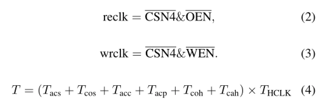
As shown in Fig.3 and Fig.4,when referring to the data input and output,they work in different ways.While the FIFO is controlled by the reading and writing clocks,the SROMC is controlled through the reading and writing control signals. Therefore,we have to convert the reading and writing control signals of the SROMC into reading and writing clocks for the FIFO.After the study and some analysis,the following logic formula is available for conversion:

Special attention should be paid to synchronization of“rdclk”and“wrclk”signals by the system clock to avoid conf l ict in the sequential circuit.As the system clock frequency of the FPGA is 50MHz,the cycle of the rdclk and wrclk signals has to be more than 40ns for synchronizing[11,12].For example, in Fig.4,as the frequency of the clock HCLK is 133MHz,we set the value ofTacpto 0,value ofTacs,Tcos,TcohandTcahto 1and the value ofTaccto 3.Thus,the cycle of the rdclk and the wrclk is 53ns according to Eq.(4).Additionally,the SROMC has different control mode,and in the page control mode,Tacpis used to read data circularly.And if the SROMC is set to the normal mode,Tacpwill be inactive or ineffective.In such a conf i guration,we can convert the reading and writing signals to reading and writing clocks for the FIFO.

Fig.3.Timing block diagram of the FIFO.

Fig.4.Timing block diagram of the SROMC in the ARM(the times are set as follows:Tacp=0;Tacs=1,Tcos=1,Tcoh=1,Tcah=1;Tacc=3).

Fig.5.Reading clock of FIFO.
However,because the data bus and address bus of the ARM are shared by the FIFO and the other devices.We must check the CSN signal before any reading and writing operation.Otherwise,the reading or writing logic will deliver a wrong result and the whole system will crash.Fig.5 shows a rdclk signal obtained from the FPGA with the help of this logic.
B.Design of the driver for the ARM
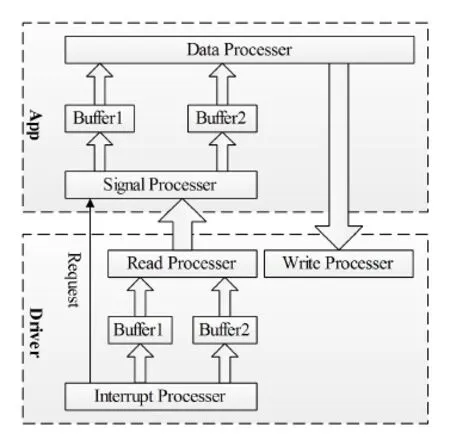
It is common that the event signal is generatedrandomly and casually when we carry on a nuclear physics experiment.So the PDAQ system cannot f i gure out when to read data.In order to solve this problem,the interrupt mechanism is implemented in the system to achieve eff i cient outcomes[13,14].It works as follows:the FPGA is set to notify the ARM to read data when the cumulative number of the event(Multi-Event mode) reaches preset value.In view of the fact that this method can reduce the burden of the ARM,the driver is expected to process the interrupt signal and notify the applications to deal with it.Fig.6 shows the driver and the application architecture of the ARM.

Fig.6.Driver and Application architecture.
The interrupt processer module is used to respond to the hardware interrupts[15].If the number of the data reaches preset value,the FPGA will transmit an interrupt message to the ARM to read the data and write it into a buffer.Further-more,in order to decrease the rate of event losses and the dead time(the time within which a second pulse is not detected), we apply the ping-pong buffer technology in the driver[16]. While the application program(APP)is reading data from one of the two buffers,the interrupt service routine can respond to the hardware interrupt,and write the data into the other buffer at the same time.Besides that,the APP in the ARM is based on multi-threading,so the signal and the data can be processed in different threads.The signal processing thread is occupied to respond to the data reading requirement from the driver,and to write the data into the APP buffer,whilst the data processing thread is used to analyze the data got by signal processing thread.Similarly,the ping-pong buffer technology is also applied in the APP.Thus,it can reduce the risk of the dead time and increase the throughput of the data.

Fig.7.(Color online)The energy spectrum of Na22.
V.EXPERIMENTS AND RESULTS
The PDAQ system achieved using the high-speed data transmission method has been tested in the following two experiments.
Firstly,in laboratory,P1010,a NIM module using to generate pulse and gate,is used to produce two kinds of signals,the pulse signal and the gate signal.The pulse signal generated is sent to the PDAQ system directly.The gate signal is processed f i rstly by GG8000,which is also a NIM module,before it is sent to the system.The experimental results shows that the maximal data transmission rate is about 2MB/s,and the frequency of the event generation is 250kHz.
In the second experiment,the PDAQ system is applied to process the energy spectrum of Na22radioactive source using LaBr3detector.The energy-signal was converted to the pulse signal and the gate signal after it is amplif i ed by photomultiplier of the detector.Experimental results illustrated in Fig.7 showed that the energy spectrum acquired by using this PDAQ system is the same as that obtained through PHILLIPS7164.
VI.CONCLUSION
Thehigh-speedtransmissionmethodsuccessfullysolvedthe problem that massive data is dif fi cult to be transmitted in highspeed between FPGA and ARM in the PDAQ system.The fi rst realistic experimental results show that the maximal data transmission rate can reach 2MB/s,and the rate of event generation is 250kHz.The second energy spectrum test illustrates that this method can meet the requirement of the PDAQ system.However,as a result of some tiny fl aw from the other parts in the system,the whole system cannot run at the speed of 8MB/s.Once all the parts of the system are completed,the system can run at full speed.
[1]Wang Y Y and Ma X L.Nucl Electron Detect Technol,2007,27:18–19.
[2]Hao J,Ojaruega M,Becchetti F D,et al.Nucl Instrum Meth A, 2011,652:483–486.
[3]Lu W,Cheng Z Q,Kong J,et al.Nucl Phys Rev,2012,28:464–468.
[4]Kong J,Su H,Chen Z Q,et al.Nucl Instrum Meth A,2010,622: 215–218.
[5]Monica T,Jon A,Micrea B,et al.Phys Procedia,2012,37: 1940–1947.
[6]BauerDA,BurkeS,CooleyJ,etal.NuclInstrumMethA,2011,638:127–133.
[7]He Q,Tang B,Du D M,2009 International Conference on Measuring Technology and Mechatronics Automation,2009,370–373.
[8]Liao Y K.ARM and FPGA design and application,China electric power press(in Chinese):238–240.
[9]Shen H and Wang Y X.Aeronaut Comp Tech,2007,37:109–111.
[10]Zhu X P,Xiao T J,Zhao H,et al.Comp Eng Des,2009,30: 3088–3090.
[11]Liu J,Yang Y,Yu X Z.Mod Electron Tech,2007,20:182–186
[12]Zhang Q.Research and Exploration in Laboratory,2003,22: 47–49
[13]Zhang J C,Wang Y Y,Nan G Y,et al.High power laser and particle beams,2012,24:2727–2730.
[14]Nan G Y,Wang Y Y,Zhang Y C.Nucl Electron Detect Technol, 2011,31:1250–1254.
[15]Corbet J,Rubini A,Kroah-Hartman G.Linux device drivers, China electric power press(in Chinese):46–74.
[16]Li W S,Chi Z Y,Chen W J.Optoelectronic Technology and Information,2005,18:76–79.
10.13538/j.1001-8042/nst.25.010404
(Received July 24,2013;accepted in revised form December 20,2013;published online February 20,2014)
∗Corresponding author,yanyu@impcas.ac.cn
杂志排行
Nuclear Science and Techniques的其它文章
- Using activation method to measure neutron spectrum in an irradiation chamber of a research reactor∗
- A neural network to predict reactor core behaviors∗
- Research on GPU-accelerated algorithm in 3D f i nite difference neutron diffusion calculation method∗
- Development of a three dimension multi-physics code for molten salt fast reactor∗
- Performance simulation and structure design of Binode CdZnTe gamma-ray detector
- Effectiveness and failure modes of error correcting code in industrial 65 nm CMOS SRAMs exposed to heavy ions∗
