ZnSe掺Cu与Zn空位缺陷的稳定性、电子结构与光学性质
2012-12-11张胜涛
郭 雷 胡 舸 张胜涛
(重庆大学化学化工学院,重庆400044)
ZnSe掺Cu与Zn空位缺陷的稳定性、电子结构与光学性质
郭 雷 胡 舸*张胜涛
(重庆大学化学化工学院,重庆400044)
采用基于密度泛函理论框架下的第一性原理平面波超软赝势方法,对ZnSe闪锌矿结构本体、掺入p型杂质Cu(Zn0.875Cu0.125Se)及Zn空位(Zn0.875Se)超晶胞进行结构优化处理.计算并详细分析了缺陷体系的形成能和三种体系下ZnSe材料的态密度、能带结构、集居数、介电和吸收光谱.结果表明:在Zn空位与Cu掺杂ZnSe体系中,由于空位及杂质能级的引入,禁带宽度有所减小,吸收光谱产生红移;单空位缺陷结构不易形成, Zn0.875Se结构不稳定,Cu掺杂ZnSe结构相对更稳定.
硒化锌;空位缺陷;Cu掺杂;电子结构;光学性质;第一性原理
1 Introduction
Zinc selenide(ZnSe)is an II-VI semiconductor material with a relatively wide and direct band-gap(2.67 eV at room temperature)and high optical transparency(~90%).1It has high potential and attraction for optoelectronic applications such as green-blue light emitting diodes,laser diodes,and solar cells etc.2-4In order to design novel semiconductor materials,considerable theoretical and experimental efforts have been devoted to determine the electronic and optical properties of ZnSe system materials.5-7Moreover,ZnSe is experiencing a renaissance as a material with properties most appropriate for application in quantum computing.Recently,Yamamoto et al.8have shown that independent ZnSe quantum wells doped with fluorine can emit indistinguishable photons,which can be used to encode and transport information.Jana et al.9synthesized Cu(II)doped ZnSe nanoparticles using molecular cluster precursors.The Cu(II)dopant had the effect of quenching the ZnSe band edge emission,yet only weak emission from Cu(II) centers was observed.However,very little is known about the microscopic structure of Cu-related point defects in ZnSe.As far as we know,a native point defect in ZnSe that has been positively identified is the zinc vacancy.This defect was also observed in electron-irradiated ZnSe at low temperatures by Watkins,10who considered that the neutral zinc vacancy had a threefold-degenerate level in the band gap(with a capacity of six electrons),four of which are occupied.
Although experimenters have tried their best to realize the high quality p-type ZnSe conductivity via introducing probable dopants,the origin of the doping difficulties remains unclear. In order to contribute to a better understanding of defect mechanism,we performed density functional calculations on zinc vacancy and Cu-related point defects in ZnSe.In the present article,the formation energies,electronic and optical properties of the defects have been calculated.The band structure,density of states,Mulliken charges,dielectric functions,and absorption spectra were analyzed in terms of the precisely calculated results.
2 Methods and models
2.1 Computational details
All calculations were performed using the plane-wave pseudopotential approach and the generalized gradient approximation(GGA)within Perdew-Burke-Ernzerhof scheme as implanted in CASTEP.11Zn 3d104s2,Se 4s24p4,and Cu 3d104s1were treated as valence states because of their relatively high energies.In all calculations,self-consistency was achieved with a tolerance in the total energy of at least 1.0×10⁻⁵eV· atom-1.The lattices and the positions of the atoms were fully relaxed to minimize the total energy with all the forces on the atoms converged to less than 0.1 eV·nm-1.The cutoff energy was 400 eV,and a 4×4×4 k-points grid was adopted for integration in the first Brillouin zone.The total stress tensor was reduced to the order of 0.02 GPa using the finite basis set corrections.Optical properties may be determined using the complex dielectric function ε(ω)=ε1(ω)+iε2(ω).12The imaginary part of the dielectric function is given as:

The real part of the dielectric function can be evaluated from the imaginary part by applying the Kramers-Kronig relations:

where C and V denote the conduction band(CB)and valence band(VB),corresponding to the intrinsic energy EC(k)and EV(k),|e·MCV(k)|is the momentum operator,e is the electronic charge,ω is the light frequency,k is the reciprocal lattice vector.The peaks appearing in the ε2(ω)part of dielectric function are directly related to different intra-band or inter-band transitions in the first irreducible Brillouin zone.The absorption spectrum is calculated using Eq.(3).13

The calculation of optical properties usually requires a dense mesh of uniformly distributed k-points.We employ Brillouin zone integration with a 20×20×20 grid of Monkhorst-Pack points for the calculation.
2.2 Models
Ideal ZnSe in cubic zinc-blende(ZB)structure belongs tospace group,T2dsymmetry system.The primitive cell contains four zinc(Zn)cations and four selenium(Se)anions,and the cell parameters are a=b=c=0.5668 nm,α=β=γ= 90°.All configurations were simulated within a ZnSe supercell,being equivalent to a 2×1×1 primitive cell and containing 16 atoms,with periodic boundary conditions applied.Using the similar tactics,14,15when doping or creating vacancy,the Zn [0.5,0.5,0.5]atom would be directly substituted by Cu atoms or removed.Besides,depending on the circumstances,we divide Se atoms into two categories:Se I(Se1-Se4)and Se II (Se5-Se8),and four groups for Zn atoms:Zn I(Zn1,vertex atom),Zn II(Zn2,midpoint atom),Zn III(Zn3,centroid atom), and Zn IV(Zn4-Zn7),as displayed in Fig.1.
3 Results and discussion
3.1 Structural properties
Firstly,the three periodic supercells of ZnSe were optimized for testing the validity of the method.
Table 1 summarizes the equilibrium lattice constants of pure and defective ZnSe systems.Our calculation for pure ZnSe is slightly beyond the experimental value.16This overestimation of the lattice constants based on the GGA method is reasonable.17However,it is in good agreement with other theoretical result.18A little bigger for Zn0.875Se in volume than pure ZnSe derived from weaker interactions between the hole and surrounding atoms.Conversely,the volume reduction for Zn0.875Cu0.125Se results from a minor difference in atomic radius between Cu and Zn.The local structure around the Cu dopant is slightly suppressed with the Se atoms drawn closer to the Cu atom after geometry optimization,for which evidence can be found in Table 2.
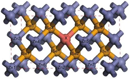
Fig.1 Supercell structure(2×1×1)of ZnSe with defectX:vacancy or impurity atom

Table 1 Optimized geometric lattice parameters of perfect and defective ZnSe systems
Zn atoms and Se atoms contributed four bonding electrons to form a polar covalent bond normally.The removal of Zn atom from the perfect ZnSe causes structural relaxations of the ions surrounding the vacancy.Four bonding electrons are removed while the formation of Zn vacancy,such a close neighbor of the vacancy of the Se atoms will appear four effective charge of dangling bonds.Unsaturated bonds are thus reconfigured because of the electronic resonance coupling among dangling bonds with the nearest neighbors and the second nearest neighbors.Fig.2 provides the differences of charge density of study subjects around Zn-vacancy and Cu-impurity.Compare Fig.2(b,c)to Fig.2(a),which shows that the charge density of Se atoms close to Zn vacancy is significantly reduced,and the charge density of Cu d orbitals is tiny.The charge redistribution can be seen as the micro-explanation for the above lattice distortions.
3.2 Formation energy of the defects
The formation energy(represented by Ef)is a key quantity charactering the properties of a defect or impurity in a solid, and defects with low formation energies are easy to form.For neutral defects,we calculate the defect formation energy as19,20

where Edefis the energy of the defective supercell,Ebulkis the energy of the ideal crystal cell(bulk),and nαis the number of atoms of species α that is added to(negative)or removed from (positive)the ideal crystal to create the defect,with the corresponding chemical potential μα.
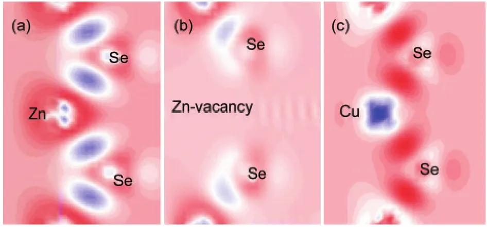
Fig.2 Plots of differences of charge density contour of(a)perfect ZnSe,(b)Zn0.875Se,and(c)Zn0.875Cu0.125Se
The chemical potentials for Zn and Se are not uniquely determined by the total energy,but depend on the crystal growth conditions.Some boundaries can be established for these chemical potentials.The energy condition gives us μZn+μSe=EZnSe, where EZnSeis the total energy of a pair of atoms in the crystal. To prevent pure Zn formation,μZn≤μZn(bulk),where μZn(bulk)is the total energy per atom of bulk Zn in a hexagonal closepacked structure.The upper limit of the Zn chemical potential for the zinc-rich limit in ZnO meets μZn=μZn(bulk).We must also have μSe≤μSe(bulk),otherwise bulk Se would be more stable than the ZnSe crystal and precipitation would occur,forming a bulk Se phase.Limited by the thermodynamic stability condition for ZnSe,μZnand μSeare variables correlated as:

where ΔH(ZnSe)is the enthalpy of formation of bulk ZnSe. The calculated formation enthalpy of ZnSe is-6.14 eV,in good agreement with experimental values.21Under the Zn-rich limit condition,μZn=EZn,μSe=ΔH(ZnSe)-EZn;similarly,under the Se-rich limit condition,μSe=ESe,μZn=ΔH(ZnSe)-ESe.Particularly,we have used the bulk fcc Cu as the source of the Cu atom.The formation energy of the zinc vacancyis 4.26 eV (3.34 eV)under the Zn-rich(Se-rich)condition,while that of the Cu defectis-2.13 eV(-1.21 eV)under the same condition.is so high that it is hard to create VZnin bulk ZnSe.However,if a Zn vacancy is accompanied by a Li(or H) interstitial,its formation energy can be sharply lowered.22A negative binding energy of Cu impurity means that the reaction is exothermic,can be fabricated more easily by experiments and more stable than anion-doped ZnSe with typically positive formation energy.23
3.3 Electronic structures
Fig.3(a-c)show electronic band structures along the symmetry lines of the Brillouin zone for ZnSe,Zn0.875Se,and Zn0.875Cu0.125Se,respectively.The energy scale was measured in eV and the top of the VB was set to zero on this energy scale. It is obvious that the valence band maximum(VBM)and conduction band minimum(CBM)occur at the same k-point(G) for all the three cells,indicating that they are all direct gap semiconductors.However,the calculated band gap of ZnSe isabout 1.747 eV,only 65.2%of the experimental data,24but agrees well with the value reported by Laref et al.25The severe underestimation of semiconductor band gaps is a well-known drawback of LDAand GGA.26

Table 2 Mulliken bond population analysis of Zn―Se and Cu―Se bonds

Fig.3 Band structures in the vicinity of the Fermi level(a)perfect ZnSe,(b)Zn0.875Se,(c)Zn0.875Cu0.125Se;The Fermi level was indicated by the dot line.
Fig.4(a-c)show the density of states(DOSs)of perfect ZnSe,Zn0.875Se,and Zn0.875Cu0.125Se,respectively.The DOSs in Fig.4(a)indicate that CBs of ZnSe originate mainly from the cooperative contributions of Se 4p,Zn 4s,and Zn 3d orbitals, among which Zn atoms are dominant.VBs between-13.5 and-11.5 eV are derived from Se 4s orbital.This band is somewhat isolated and far away from the other bands that we will pay little attention on it.The major contributions to VBs between-7.5 and-5.0 eV are mainly from Se 4p and localized Zn 3d orbitals.The upper VBs from-5.0 to 0.0 eV are mostly composed of Se 4p states.
However,compared with those of perfect ZnSe,Se 4p states of Zn0.875Se shift to upper energy range and vacancy orbitals appears in the vicinity of the Fermi energy.It is caused by the lone unpaired valence electrons of Se atoms.Those differences caused by electron deficiency will strongly affect the optical properties.The theoretical calculations have predicted that the zinc vacancy in Zn0.875Se may form shallow acceptor level and make them p-type conductivity.
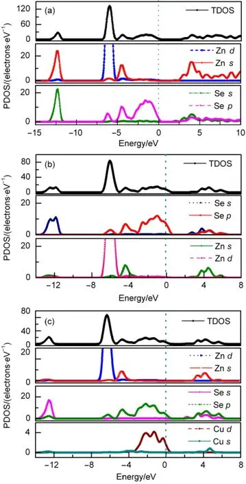
Fig.4 Total and partial state densities of(a)perfect ZnSe, (b)Zn0.875Se,and(c)Zn0.875Cu0.125SeThe zero point energy(vertical line)was aligned at the Fermi level.
Had the VBM consisted of anion orbitals alone,one would expect roughly similar band gap in ZnSe and Zn0.875Cu0.125Se, since the Cu s-orbital energies are close to those of Zn.The band structure and DOSs indicate that Zn0.875Cu0.125Se has a narrower band gap(1.537 eV),and the energy of the VBM(EV) rises to 0.239 eV,as shown in Figs.3(c)and 4(c),respectively. The appropriate explanation seems to be the p-d repulsion effect:27the Cu 3d orbitals in Zn0.875Cu0.125Se are considerably closer in energy to the Se 4p orbitals than the Zn 3d orbitals,leading to a far more effective p-d repulsion,with a consequent dramatic reduction in the band gap compounded by the fact that the Cu 3d orbitals are also more delocalized than the Zn 3d orbitals,leading to a largercoupling matrix elementin Zn0.875Cu0.125Se and,hence,a larger p-d repulsion.Fig.5 shows a schematic diagram of the p-d repulsion effects for the hypothetical ferromagnetic ZB CuSe.As we can see:the Cu 3d states split into a triply degenerate t2gstate and a double degenerate egstate,the t2gorbitals couple with the Se 4p orbitals to form bonding states(B+or B-)and antibonding states(AB+or AB-), but the egorbitals of Cu have no counterpart in Se and hence remain nonbonding.The downward shifting of the lowest-lying CB energy arises from the strong sp hybridization between Cu 4s orbitals and Se 4p orbitals.28Zn0.875Cu0.125Se produces a deep acceptor impurity level from the EV,resulting in the lower concentration of the holes,which need larger ionization energy. This may be one of the foremost difficulties in p-type doping.
As a comparison,we calculated crystal orbital overlap populations for the three systems on the grounds that this helps to understand bonding behavior,as listed in Table 2.In addition to providing an objective criterion for bonding between atoms, the overlap population may be used to assess the covalent or ionic nature of a bond.29A high value of the bond population indicates a covalent bond,while a low value indicates an ionic interaction.Positive and negative values indicate bonding and antibonding states,respectively.A value for the overlap population close to zero indicates that there is no significant interaction between the electronic populations of the two atoms.30From Table 2,a large proportion of Zn―Se bond overlap population values among the three systems are high,exhibiting covalent bonding;some show mixed ionic-covalent character.As to Zn0.875Se,the overlap population of the Zn II(or Zn IV)―Se I increases,and the bond length decreases.It suggests that Zn vacancy induced changes in the bonding of the nearest neighbor Se atoms and there was increased covalency in the Zn―Se bonds,which is in good agreement with above electron density difference analysis.The Zn IV―Se II bonds in Zn0.875Se exert strong ionic abilities with the minimum population value,and it demonstrates that valence electrons of Zn IV atoms play an important role in the Zn0.875Seʹs electrical conductivity.Note that charge population of Cu―Se I bond is higher than other Zn―Se bonds in Zn0.875Cu0.125Se,and this also indicates that covalent interaction is strengthened.
In order to further explore the structural relaxation,Mulliken atomic population analysis of all the present atoms was performed,and the results are listed in Table 3.As is clear from Table 3,the charge distributions of the same atoms are diverse along with different atom sites.In Zn0.875Se,the Se atoms seemingly cannot hold onto the obtained electrons tightly,as indicated by statistics showing decreased absolute values of charge for Se atoms,whether close to the vacancy center or not,and it is noteworthy that Se I atoms decrease slightly more than others due to a lack of electronic contribution of Zn atom.The charge value of Zn I atom increases,while greatly reduces for Zn II atom,as has been already pointed out,resulting from the unpaired valence electrons of Se atoms caused by Zn vacancy, for which evidence can be found in the abnormal increase of Zn II s orbital electron occupancy.For Zn0.875Cu0.125Se,the Se I charge changes sharply,the charge of Cu is negative(-0.06e), indicating that the electronegativity of Cu is bigger than Zn, consequently,it is more difficult to lose electrons.Obviously, whether in Zn0.875Cu0.125Se or Zn0.875Se,Zn II atoms invariably have the fewest charges,which indicates that the Zn II site has the most sensitive response to Zn vacancy or impurity atom, and the weak interactions with other neighbors would exist spontaneously.
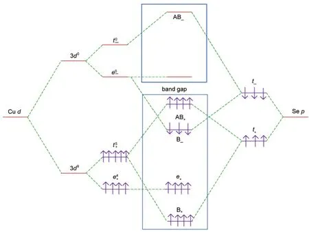
Fig.5 Schematic diagram of the p-d repulsion effects for hypothetical ferromagnetic ZB CuSe
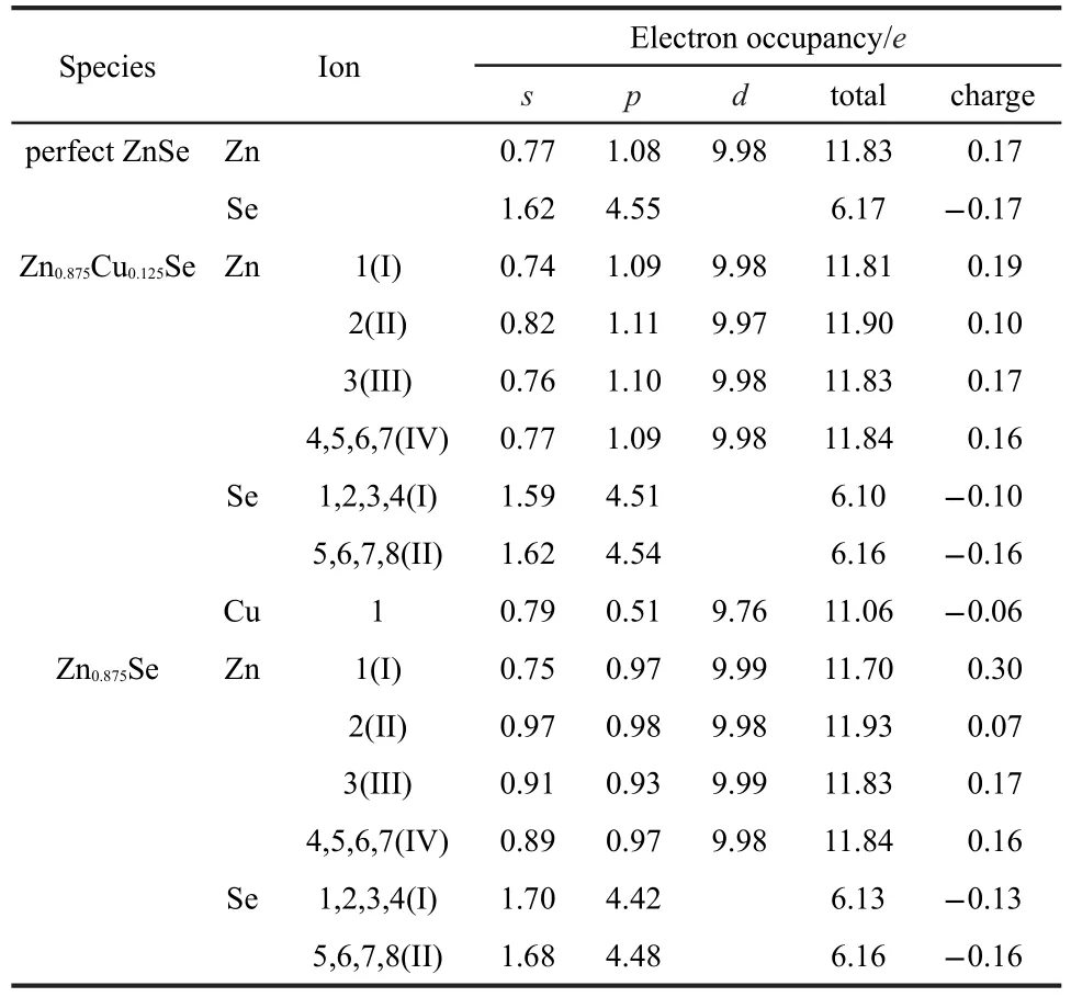
Table 3 Mulliken atomic population analysis of Zn,Se,and Cu atoms
3.4 Optical properties
The optical properties are important for these compounds, since they can find potential applications in photoelectron devices and the semiconductor industry.We amended band gaps by using a scissor operator(scissor:0.923 eV).Fig.6(a)depicts the calculated imaginary parts of dielectric function for the studied compounds.The imaginary part ε2(ω)of the dielectric function for perfect ZnSe has four prominent peaks:A(3.8 eV),B(5.3 eV),C(6.8 eV),and D(8.9 eV).Peak A mainly corresponds to the transition from Se 4p VBs to the unoccupied CBs.Peak B primarily originates from the transition from Zn 3d and Se 4p VBs to Se 4p or Zn 4s CBs,for which evidence can be found in the partial density of state(Fig.3(a)). Peaks C and D are assigned to the transition of inner electrons from Se 4s orbitals to the Zn 3d or Se 4p VBs.As to Zn0.875Se,a new peak(E)occurs at 1.8 eV,which may belong to the electron transition from CBs to vacancy acceptor level and cause emission of the red photoluminescence.Similarly,the dielectric peak F(2.0 eV)of Zn0.875Cu0.125Se is attributed to the electron transition from CBs to acceptor impurity level near by the top of VBs.
The corresponding linear absorption spectrograms are illustrated in Fig.6(b).The absorption edge of pure ZnSe starts at about 2.65 eV,in approximate agreement with the experimental data.24This originates from the transition from Se 4p electron states located at the top of the VBs to the empty Zn 3d electron states that dominate the bottom of the CBs.According to the results of calculated dielectric function,the energy of each absorption peak is almost due to the transition of electron excitation from the VBs to the CBs.Obviously,the absorption peaks show a significant redshift for both Zn0.875Se and Zn0.875Cu0.125Se.
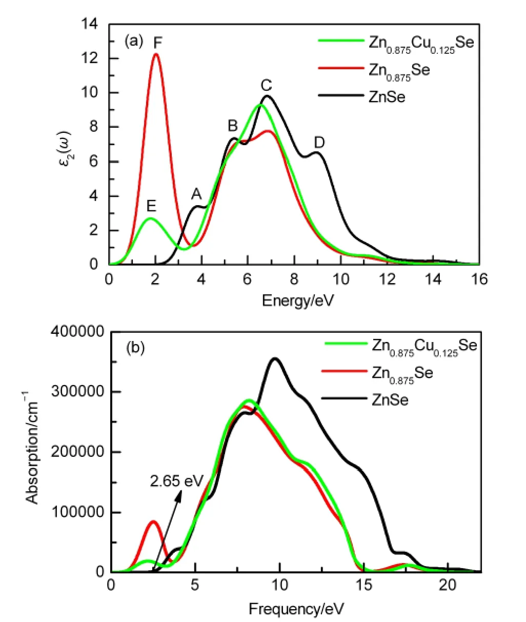
Fig.6 (a)Calculated imaginary parts of dielectric function,(b) optical absorption coefficients for ZnSe,Zn0.875Se,and Zn0.875Cu0.125Se
4 Conclusions
We have applied the GGA within the framework of plane-wave pseudopotential DFT method to investigate the defects energetics,electronic and optical properties of pure and deficient ZB structures of ZnSe.The results obtained are consistent well with other theoretical results and the available experimental data.
The results reveal that zinc vacancy increases the lattice constants and cell volume,but Cu-doping is on the contrary,yet both acceptor states on the top of valence band,providing p-type conductance.
By comparison,Zn0.875Cu0.125Se system is relatively more stable than Zn0.875Se system owing to its similar structure with pure ZnSe.The deep acceptor levels indicate that Cu-doped and zinc vacancy ZnSe systems are not easily ionized at working temperatures.But fortunately,due to the introduction of the defect level,the band gap is reduced and electronic transition in the visible region is obviously enhanced.As for Zn0.875Cu0.125Se,the p-d repulsion effect on top of valence band and sp hybridization in the bottom of the conduction band both take positive effects on band gap narrowing.
(1) Lakshmikumar,S.T.;Rastogi,A.C.Thin Solid Films 1995, 259,150.doi:10.1016/0040-6090(94)06433-4
(2)Yakimovich,V.N.J.Cryst.Growth 1999,198,975.doi: 10.1016/S0022-0248(98)01060-4
(3) Philipose,U.;Yang,S.;Xu,T.;Ruda,H.E.Appl.Phys.Lett. 2007,90,063103.doi:10.1063/1.2457190
(4) Colli,A.;Hofmann,S.;Ferrari,A.C.;Martelli,F.;Rubini,S.; Ducati,C.;Franciosi,A.;Robertson,J.Nanotechnology 2005, 16,S139.doi:10.1088/0957-4484/16/5/001
(5) Zhu,Y.;Zhang,S.H.;Zhang,X.Y.;Hao,A.M.;Zhang,S.L.; Yang,F.;Yang,J.K.;Liu,R.P.Comp.Mater.Sci.2011,50, 2745.doi:10.1016/j.commatsci.2011.03.037
(6) Desgardin,P.;Oila,J.;Saarinen,K.;Hautojarvi,P.;Tournie,E.; Faurie,J.P.;Corbel,C.Phys.Rev.B 2000,62,15711.doi: 10.1103/PhysRevB.62.15711
(7) Gundel,S.;Faschinger,W.Phys.Rev.B 2002,65,035208.doi: 10.1103/PhysRevB.65.035208
(8) Sanaka,K.;Pawlis,A.;Ladd,T.D.;Lischka,K.;Yamamoto,Y. Phys.Rev.Lett.2009,103,053601.doi:10.1103/PhysRevLett. 103.053601
(9) Jana,S.;Srivastava,B.B.;Acharya,S.;Santra,P.K.Chem. Commun.2010,46,2853.doi:10.1039/b925980e
(10) Watkins,G.D.Phys.Rev.Lett.1974,33,223.doi:10.1103/ PhysRevLett.33.223
(11) Segall,M.D.J.Phys.:Condens.Matter 2002,14,2597.
(12)Zhang,Z.Y.;Yang,D.L.;Liu,Y.H.;Cao,H.B.;Shao,J.X.; Jing,Q.Acta Phys.-Chim.Sin.2009,25,1731.[张子英,杨德林,刘云虎,曹海滨,邵建新,井 群.物理化学学报,2009,25, 1731.]doi:10.3866/PKU.WHXB20090819
(13) Feng,J.;Xiao,B.;Chen,J.C.;Zhou,C,T.;Du,Y.P.;Zhou,R. Solid State Commun.2009,149,1569.doi:10.1016/j.ssc. 2009.05.042
(14) He,K.H.;Yu,F.;Ji,G.F.;Yan,Q.L.;Zheng,S.K.Chin.J. High Pressure Phys.2006,20(1),57.[何开华,余 飞,姬广富,颜其礼,郑澍奎.高压物理学报,2006,20(1),57.]
(15) Li,J.H.;Zeng,X.H.;Ji,Z.H.;Hu,Y.P.;Chen,B.;Fan,Y.P. Acta Phys.Sin.2011,60,057101.[李建华,曾祥华,季正华,胡益培,陈 宝,范玉佩.物理学报,2011,60,057101.]
(16)Liu,C.Y.;Wang,T.;Zha,G.Q.;Gu,Z.;Jie,W.Q.J.Mater.Sci. Technol.2012,28,373.doi:10.1016/S1005-0302(12)60070-X
(17) Fan,S.W.;Yao,K.L.;Liu,Z.L.Appl.Phys.Lett.2009,94, 152506.doi:10.1063/1.3120277
(18) Shakir,M.;Kushwaha,S.K.;Maurya,K.K.; Bhagavannarayana,G.;Wahab,M.A.Solid State Commun. 2009,149,2047.doi:10.1016/j.ssc.2009.08.021
(19)Han,D.;West,D.;Li,X.B.;Xie,S.Y.;Sun,H.B.;Zhang,S.B. Phys.Rev.B 2010,82,155132.doi:10.1103/PhysRevB. 82.155132
(20) Reuter,K.;Stampfl,C.;Scheffler,M.In Handbook of Materials Modeling,Part A Methods;Springer:Berlin,2005;pp 149-234.
(21) Dean,J.A.Langeʹs Handbook of Chemistry,14th ed.; McGraw-Hill:New York,1992;p 686.
(22) Gao,H.X.;Xia,J.B.J.Appl.Phys.2012,111,093902.doi: 10.1063/1.4707888
(23)Kwak,K.W.;Vanderbilt,D.;Kingsmith,R.D.Phys.Rev.B 1995,52,11912.doi:10.1103/PhysRevB.52.11912
(24) Prete,P.;Lovergine,N.;Petroni,S.;Mele,G.;Mancini,A.M.; Vasapollo,G.Mater.Chem.Phys.2000,66,253.doi:10.1016/ S0254-0584(00)00317-5
(25) Laref,A.;Sekkal,W.;Laref,S.;Luo,S.J.J.Appl.Phys.2008, 104,033103.doi:10.1063/1.2961311
(26) Muscat,J.;Harrison,N.M.Phys.Rev.B 1999,59,15457.doi: 10.1103/PhysRevB.59.15457
(27)Wei,S.H.;Zunger,A.Phys.Rev.B 1988,37,8958.doi: 10.1103/PhysRevB.37.8958
(28)Yan,H.Y.;Li,Y.Q.;Guo,Y.R.;Song,Q.G.;Chen,Y.F. Physica B 2011,406,545.doi:10.1016/j.physb.2010.11.035
(29) Mulliken,R.S.J.Chem.Phys.1955,23,1833.doi:10.1063/ 1.1740588
(30) Segall,M.D.;Shah,R.;Pickard,C.J.;Payne,M.C.Phys.Rev. B 1996,54,16317.doi:10.1103/PhysRevB.54.16317
August 22,2012;Revised:October 8,2012;Published on Web:October 8,2012.
Defects Energetics,Electronic Structure and Optical Properties of Cu-Doping and Zn Vacancy Impurities in ZnSe
GUO Lei HU Ge*ZHANG Sheng-Tao
(College of Chemistry and Chemical Engineering,Chongqing University,Chongqing 400044,P.R.China)
Based on the first-principles within the density functional theory,the geometric structures of perfect zinc blend ZnSe,that with Zn vacancies(Zn0.875Se)and Cu-doped ZnSe(Zn0.875Cu0.125Se)were optimized using the plane-wave ultrasoft pseudopotential method.The defect formation energy,band structure,density of states,Mulliken charges,and optical spectra were calculated and discussed in detail. The results demonstrated that in Zn0.875Se and Zn0.875Cu0.125Se systems,because of the introduction of the vacancy acceptor level or acceptor impurity level,the band gap is reduced,and the absorption peaks show a remarkable redshift.Cu doping into the ZnSe system was found to be relatively stable,while the monovacancy system was not.
ZnSe;Vacancy defect;Cu doping;Electronic structure;Optical property; First-principles
10.3866/PKU.WHXB20121083
∗Corresponding author.Email:cqhuge@163.com;Tel:+86-23-65106756.
The project was supported by the Fundamental Research Funds of the Central Universities,China(CDJZR11220003).
中央高校基本科研业务费(CDJZR11220003)资助项目
O641
